

Leave it to Bill Chen, ASE, to set an optimistic tone for the 2021 Global Business Council Spring Meeting. It was exactly what the packaging community needed to hear.
The last time many of us met in person at an industry event was at the 2020 IMAPS Device Packaging Conference and Global Business Council. We had all hoped that by March 2021, we would be gathering again in Fountain Hills, AZ for these co-located events. But that was not to be.
The airwaves were crackling with nostalgia as we gathered virtually once again and tried to make the best of it. So when Chen cranked up Bob Dylan’s, The Times They are a Changin’, I could picture us all swaying arm in arm, singing along. The chatbox started filling with comments thanking him for playing it, and what a great song it is… But I’m getting ahead of myself.
The Semiconductor Times Are A-Changing
In his opening remarks, Lee Smith said that nobody expected the importance digital communications would have on our lives. We will likely remember 2020 as the year the semiconductor industry was brought to the forefront.
As scary as last year was, with the pandemic and so much illness and death, Chen pointed out the acts of individual heroism and sacrifice, and collective resilience we’ve displayed. He said the rapid development and deployment of the vaccine demonstrated “tremendous achievements in global collaboration.”
Chen presented the semiconductor news of the world, citing TSMC’s impending gigafab in Arizona, nVidia’s acquisition of ARM, AMD’s acquisition of Xilinx, Intel’s IDM 2.0 strategy, President Biden’s inclusion of $50B for R&D semiconductor spending, the White House convening a summit to address the automotive chip shortage and more. All this, he says provides proof of our changing industry landscape that will affect our industry and its eco-economics.
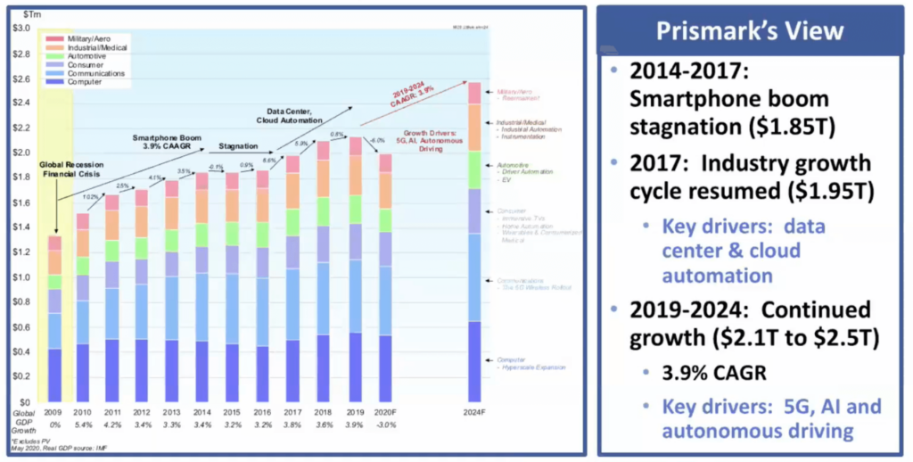
“Technology companies are leading the digital transformation of the global economy and fueling the AI revolution,” said Chen (Figure 1).
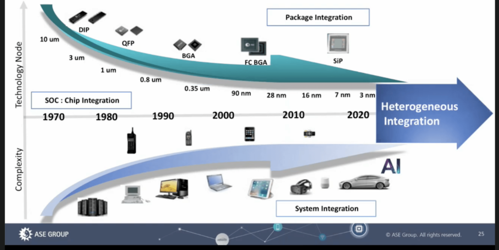
He cited a talk, “The Future is System integration” by Prof. Philip Wong, of TSMC, who remarked that as we need the end of Moore’s Law, it’s like coming out of a tunnel into green fields and sunlight. Following Moore’s Law put us on a laser-focused path of miniaturization towards the next node. Coming out of that tunnel brings us into a broader scope, where opportunities for research and innovation abound
Using innovations such as Intel’s EMIB advanced packaging and Foveros chiplet integration, and TSMC’s SoIC, and Samsung’s X-Cube 3D wafer-level integration as examples, Chen showed how chip and system integration are converging in heterogeneous integration.
Die Stacking Update
AMD’s Bryan Black, well known for his work with die stacking and on the team that introduced the Fiji processor, focused his talk, Enabling the Transition to Heterogeneous Integration, on how to move through the challenges he’s seen with AMD products (Figure 3).
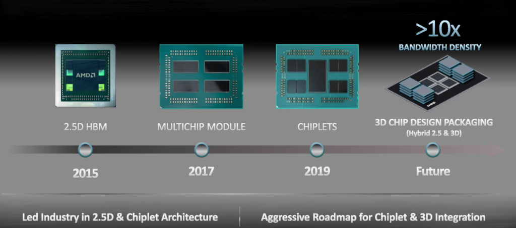
Different sources of die in the package are what makes it so challenging, he said. Developing new packaging solutions calls for creating IP for the die in parallel. “Fundamentally, there are endless configurations and complexities. This needs to be managed moving forward with heterogeneous integration,” he said.
Eliminating memory interfaces and scaling AMD’s infinity fabric will be needed going forward, he said. Bridge approaches look interesting as we outpace the capability of stitching interposers together. “We’re solving the known-good-die (KDG) issue by re-defining it as sufficiently good die.” Additionally, we’ll need new ways of testing going forward.
Black added that this can’t happen overnight but requires planned migration over a period of time. Bottom line: “Heterogeneous integration is inevitable. It will be prolific across the industry,” he said, adding that he sees challenges as opportunities to innovate across the industry.
Chiplets 101
Unimicron’s John Lau, well-known industry-wide for his years of research in advanced packaging and 3D integration, educated us on the different types of chiplet integration, providing a history lesson of different approaches. He categorizes chiplets into two categories: silicon-based, and substrate-based. He also described the difference between split chips and partitioned chips. (Figure 4).
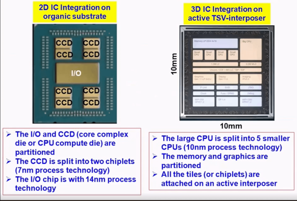
Chiplets can lead to denser chips, Lau said, depending on the approach and the substrate. Because Intel’s Foveros involves chiplets stacked on an active through silicon via (TSV) interposer, Lau considers it to be 3D IC integration.
He defines heterogeneous integration as using packaging methods to integrate different chips on an organic substrate. The advantage of the substrate vs. silicon approach is time-to-market, flexibility, fewer IP issues, and optimized signal integrity and power.
Speaking of Substrates…
Because substrates are such a broad topic, Jan Vardaman focused her remarks on high-performance computing applications. She noted that we are entering a new era of heterogeneous integration that includes 3D and chiplets, and as a result, substrates are increasing in size and layer count to meet the needs of these architectures. As the number of build-up layers increases, we need to add more substrate capacity.
While the industry’s substrate capacity is currently constrained, suppliers are concerned about adding capacity because demand could fall and drive prices down. As a result, lead times are stretched out. Vardaman noted that this fear of over-capacity happens a lot in the industry. Today. new production lines for substrates with finer feature sizes cost $300M or more per line.
Adding capacity is an expensive solution. The industry needs to come up with alternative approaches such as putting the density in the redistribution layer (RDL) by using an RDL Interposer. This reduces the number of build-up layers needed and improves yield. Samsung talked about this in the IMAPS keynote. Another way to reduce layer count is to use a Si interposer and put the density in the chip-to-chip connections. TSMC is implementing this approach with its SoIC.
Glass Substrates
Santosh Kumar, of Yole Developpement, concluded the Global Business Council meeting with an update on glass substrates. He talked about the benefits of using glass substrates for things like fan-out wafer-level packaging, microfluidics, power packaging, photonics, RF, devices MEMS actuators and sensors, CMOS image sensors, and memory.
Kumar predicted a 20% CAGR from $196M in 2019 to 2025 to $ 580M. He noted that CMOS image sensors are still the biggest market, and microfluidics is also seeing growth. Lastly, Kumar noted that the number of glass substrate suppliers continues to grow, which will help with adoption as it allows for multi-sourcing.
IMAPS DPC and the Global Business Council On-Demand
If you want to dive deeper into the details of the IMAPS DPC and Global Business Council sessions, I have good news! Registration has been extended to May 14, and all the sessions are available. And don’t forget to mark your calendars for IMAPS Symposium 2021, October 12-14, 2021, where hopefully we’ll all get together in person at the new and improved Town and Country in San Diego. I can’t wait to hug you all! ~ FvT


