
Before I could start writing my blog post about the keynote talks delivered at the 2021 Virtual IMAPS Device Packaging Conference, I first had to find out what an XPU was.
I’m often stymied by this industry’s penchant for acronyms and my journalistic need to write them out in the first instance and then use the acronym going forward. Some I’ve committed to memory – central processing unit (CPU), graphics processing unit (GPU), the newest one: network processing unit (NPU) . But I couldn’t for the life of me figure out what the “X” stands for, in XPU. Even Google tried to correct me – “Do you mean CPU?” No, Google! I mean XPU.
And then there it was: referenced in articles about both Samsung and Intel. XPU was most clearly defined in this article in Global Finance Magazine, about Pat Gilsinger’s plans for Intel.
“An XPU is a complete cross-architecture computing solution across all major chip types, all tied together in a single application programming interface, assigning each task to whichever chip is best suited to process it.” So going forward, there will be no “writing out” of XPU.
As I discovered in this article on AnandTech, Samsung Foundry and Baidu partnered back in 2018 on a AI accelerator chip based on Baidu’s XPU neural processor architecture, which uses Samsung’s “I-Cube” 2.5D interposer packaging. So, I guess the XPU term is nothing new. But in case, like me, you wondered about its origin, now you know. I expect you’ll start hearing it more and more.
An XPU is the Ultimate in Heterogeneous Integration
Both the keynote delivered by Seung Wook Yoon, of Samsung Electronics and Ram Viswanath Intel, focused on each company’s efforts in advanced packaging architectures over the years to enable heterogeneous integration.
Yoon’s talk focused on chiplet technologies. He said all types of advanced packaging from mult-chip modules (MCMs), fan-out wafer-level packaging (FOWLP), 2.5D and 3D architectures can be used to enable chiplets technology.
The most popular chiplets so far use organic substrate-based approaches, and that AMD is the most well-known for this, noted Yoon. The advantage is the ability to optimize the integration of chips, and only use advanced node technologies where they are specifically needed.
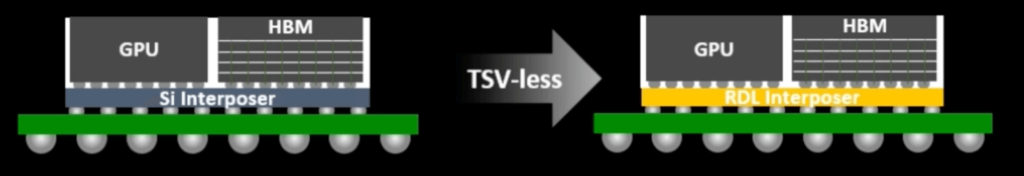
Yoon said Samsung’s is working on an RDL interposer with ultra-fine line and spacing as an alternative to its Si interposer technology to overcome the challenges brought on by chiplet architecture. Namely, it doesn’t require costly through-silicon vias or have reticle limits.
He also talked about Samsung’s X-Cube, its 3D system-in-package (3D-SiP) an industry-first 3D SRAM memory and logic stack for 5nm and 7nm node technology.

Viswanath also walked us down Intel’s Packaging Memory Lane beginning in 2013, when the company started to get really serious about heterogeneous integration (Figure 2). He said we are now at an inflection point with packaging architectures because while they provide design flexibility, they add complexity to manufacturing.
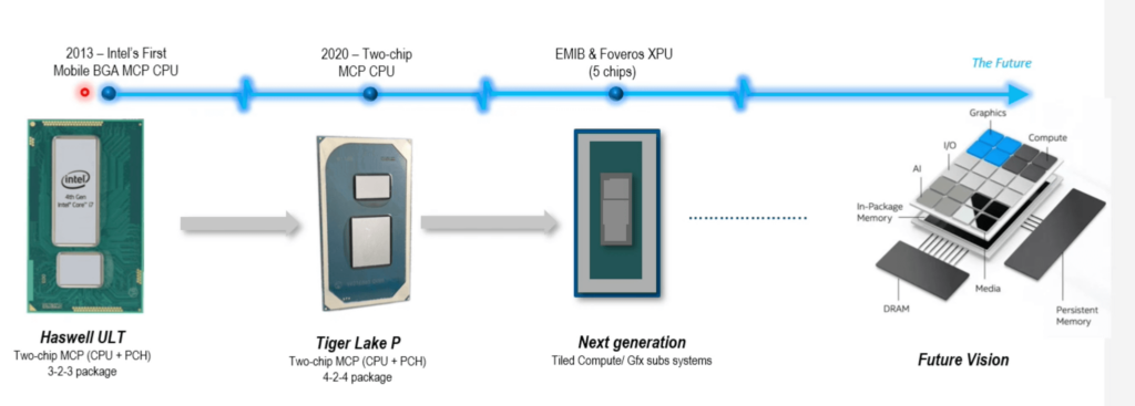
Intel’s state-of-the-art in 2020 is the Tiger Lake two-chip CPU built using both chip-on-wafer-on-substrate (CoWoS) and embedded multi-die interconnect bridge (EMIB) technology. Next-generation approaches will combine EMIB and Foveros to stack five graphics chips like tiles into an XPU. EMIB is an organic substrate approach. Foveros is a true 3D architecture in which die are stacked on an active silicon base using TSVs and solder bumps.
The vision for the future, said Visanwath, will use Foveros and EMIB to create chiplet architectures that integrate multiple functionalities into one package and will achieve finer pitches by replacing solder bumps with Cu-Cu hybrid bonding. To reach this level of complexity, he says we have to overcome some challenges, such as non-standard IO interfaces, new materials, thermal management issues, cross-domain design expertise to design from the outside in, and more.
Calls to Action: Collaboration EDA Tools and HVM Hybrid Bonding
Here’s what I found most interesting. Both Yoon and Viswanath talked about hybrid bonding as a key enabler needed to deliver next-generation versions of their technologies. Viswanath noted that while hybrid bonding processes are available, there is a lack of high-volume production tools for it, and so it will be 2-3 years before we can expect hybrid bonding to be used in Intel’s products. Both speakers also mentioned a need co-design EDA tools that take chiplet architectures into account. I might be wrong, but I think both the hybrid bonding tools and the EDA tools already exist. Did they just not get the memo? Or are they looking for capabilities beyond what’s already been developed?
In any case, Visanwath called for collaboration across the supply chain to achieve these goals. What’s the end game? “High bandwidth, extreme power efficiency, and maximum scalability at and affordable proce point. – as a community this is our holy grail,” he said.
If you missed the live event, you may still be able to register here to view it on demand. There’s more to come! ~ FvT


