

 Avi Bar Cohen 1946 – 2020
 Avi Bar Cohen 1946 – 2020
 Before we take a look at some interesting papers from the recent IMAPS 2020 Virtual Conference, I wanted to express my sadness for the loss of my colleague and dear friend, Avi Bar Cohen, who passed away on October 10, 2020. I first started working with Avi in the early 1990s when he served as Editor of the IEEE EPS (then called CHMT) journal. In his later life, when he moved to DARPA to become the Director of the ICECool program, he pulled me into DARPA and made me a packaging subject matter expert (SME). We worked on many IEEE and Govt. programs together through the years.
In all the years we worked together, I always found Avi to be a hard-working, reliable, and trustworthy individual with a great sense of humor and I will miss his presence in our advanced microelectronics community. Rest in peace Avi………
Now finishing up our look at IMAPS 2020………
IBM Japan
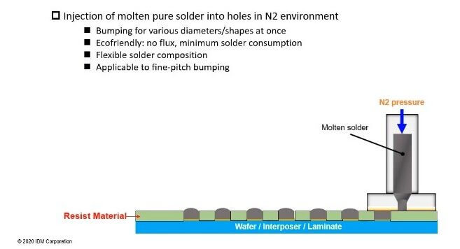
Aoki of IBM Japan reported on the development of a plating-free copper pillar bump process by combining their injection molded solder (IMS) solder deposition process with their copper nano paste printing technology. If this process can be commercialized it would eliminate the need for seed layer deposition and seed layer etch operations. The injection-molded solder process is shown in Figure 1.
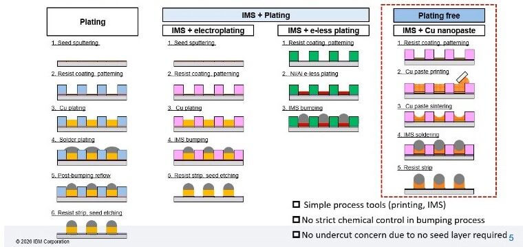
A comparison of a generic plating process vs a copper plating + IMA solder was totally plating free process ae compared in Figure 2.
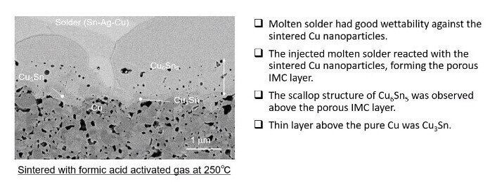
One of the goals of the program was to understand the Cu microstructure of the nanoparticle paste (80nm particles; 70 wt % copper) as it is developed under nitrogen vs formic acid /nitrogen (reducing atmosphere) at various temperatures.
They found that the formic acid promotes larger copper grains and promotes fusing of the copper particles to the copped pads of the structure. At 250°C they see larger grains but also voids. The optimized condition appears to be formic acid at 200°C.
SEM/EDX of the solder/np-Cu interface shows the expected Copper tin IMC as shown in figure 3:
YOLE Developpment
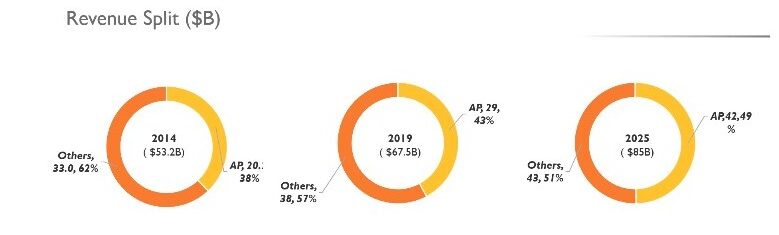
During the Yole presentation by Trivedi, they reported their projection of the advanced packaging market growing to $ 85B by 2025 (Figure 4)

Cadence
John Park of Cadence appears to be on a chiplet tour presenting at all the major conferences. At IMAPS his presentation was “Design Tools and Flows for the Chiplet Generation” It was of interest because of a couple of great slides shown below.
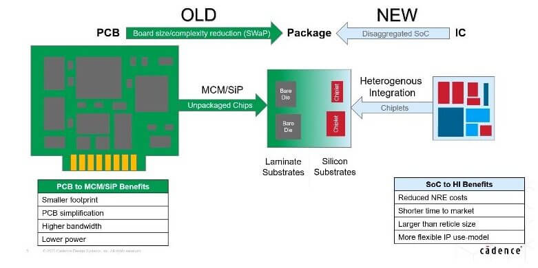
Figure 5 shows how mounting everything directly on the PCB was supplanted by MCM (later called SiPs) where chips were combined into modules. We are now seeing SoC’s broken down (IFTLE calls it disintegration) into chiplets and recombined into modules. Nice perspective and a nice explanation for those who are struggling to understand the difference.
The other key slide gives the Cadence perspective on the hurdles remaining for chiplets to fully integrate into the microelectronics infrastructure (Figure 6).
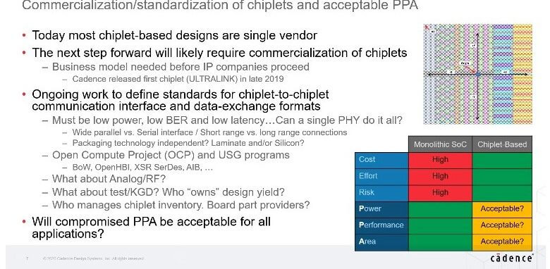
IFTLE has discussed the standardization requirements many times before and the issue is not going away. Just like stacked memory chips needed a standard (and finally got one) so does the chiplet community. Chiplets from multiple vendors must be able to communicate or this will become a niche technology used internally by the like of Intel, AMD and a few others each of whom have their own interfaces.
For all the latest in advanced packaging stay linked to IFTLE………………………………………….


