In the second great keynote presentation of the Annual IMAPS Symposium a few weeks ago [see IFTLE 465 “ Intel Reviews Leading Edge Packaging Technology”] AMD’s Bryan Black, the Godfather of chiplet technology, opined on “Chiplets: How to Utilize Them, Some of Their Challenges and What They Can Do”
Back in 2006, Black was at Intel teaching us about why one would “disintegrate” microprocessor functions and then reintegrate them into a 3D stack. In 2011, now at AMD, Black told us at the Ga Tech Interposer Conference that “….Southbridge (22 nm) is probably the last chip that will be impacted by scaling” and that in the future “… separately fabricated functionalities will be combined vertically (3D) and/or horizontally (2.5D) on an interposer to form the final circuit function” Given this background, let’s take a closer look at what Black had to say.
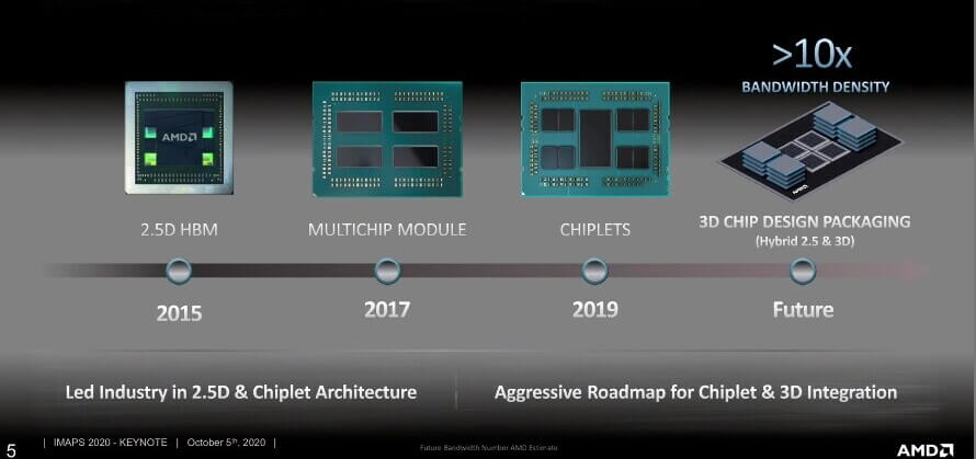
Black reported that by 2014 their focus was to break up single die SoC into what we call today chiplets. This allows one to scale functionality separately, only where it is needed. In 2015 AMD introduced Radeon graphics Fiji (above) with the first use of high bandwidth memory (HBM) stacks, which it had developed jointly with Hynix.
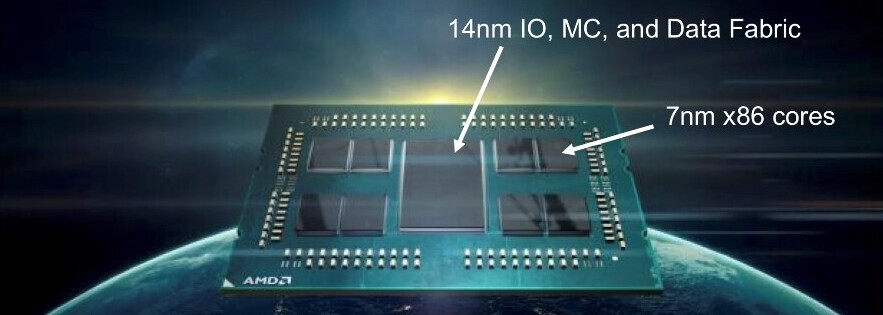
In 2018 AMD shipped its second-generation EPYC chip (Figure 1), taking a monolithic solution and divided it up into very specific functionalities. I/O, memory control, and data fabric were done on 14nm die and 7nm technology was focused on the x86 dies.
Black then indicated that its roadmap is full of 3D chiplet design solutions as shown in Figure 2.
Why Chiplets?
As Moores Law keeps slowing and die sizes keep increasing at an unsustainable rate, we are required to break up these chips to maintain yields (similar to what Xilinx taught us we had to do for FPGA chips in 2010). Using the latest node only where needed results in reduced silicon cost, These savings, in turn, can be allocated for more expensive packaging solutions.
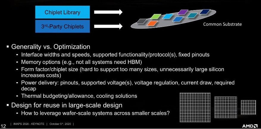
In addition, these functional chiplets will create a library and in the future we can combine these tested chiplets with other chiplets, some from 3rd parties, to devise future circuits (i.e the goal behind the DARPA CHIPS program).
Chiplet Problems:
- When using chiplets, it is unavoidable that we create memory coherency issues and “non-uniform memory latency” depending on where the memory is stored.
- Chip security used to be on the SoC die. Now using chiplets we need new security solutions
- Parametric variations – small differences in die electricals can be significant in the reassembled chiplet module. More “binning” will be required as well as other (undescribed) electrical solutions.
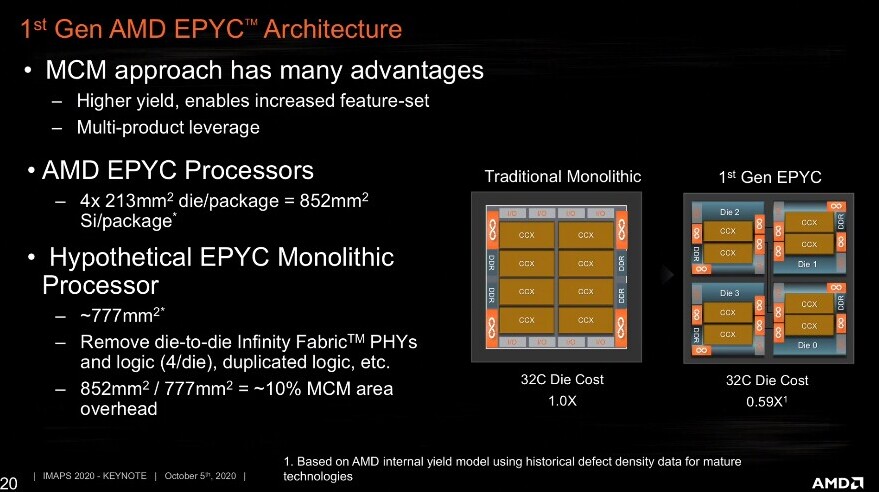
Black closed by showing EPYC solution shown below where they needed 10% more Si area but the resultant smaller die gave more die/wafer and a higher yield. The total cost of the chiplet solution was a remarkable 59% of the monolithic SoC die.
For all the latest in advanced packaging stay linked to IFTLE…………………..