
In recent blogs, we have discussed the damage done to Intel’s leading-edge technology reputation by major delays in both their 10nm and 7nm product introductions [ see IFTLE 458]. We have also seen them try to put a positive spin on the fact that they may have to go external to get 7 and 5nm chips from foundries like TSMC and Samsung to meet product requirements in a timely fashion.
At the Intel Architecture Day in mid-August, the clear overall message was that future progress in IC performance will be predicated less on node shrinks and more on architectural innovations. Long time readers now have been hearing that from IFTLE now for over a decade.
Raja Koduri, Intel’s chief architect, focused on what Intel calls the Six Pillars of Innovation which they defined as a process (which includes packaging), architecture, memory, interconnect, security, and software.
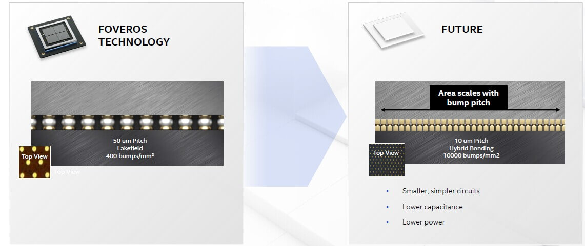
The packaging was called a critical element to put heterogeneous design elements together in an “efficient and coherent manner”. Koduri named this the “Architecture Era” noting that relying just on process shrinks as the main driver of innovation is no longer the smart way to improve system performance. Intel then relayed how they are investing in 2.5D and 3D structures and other enabling packaging technologies like fine bump pitch and hybrid bonding.
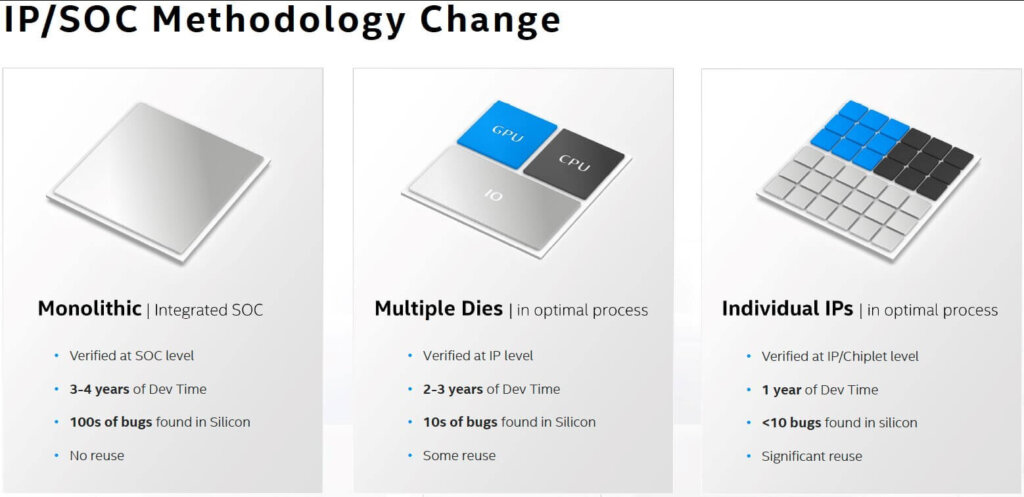
Intel’s move towards more complex packaging is shown best In the following slide where we see a major change in how devices are being architected.

One of the best summations of Intel’s packaging technology landscape was given by Babek Sabi, corporate VP and GM of their Assembly and Test Division (ATD) at his Keynote presentation “Advanced Packaging Architectures: Scaling for a Heterogeneous World” given at the Recent IMAPS conference.
Sabi points out that:
- If anything, we have underestimated the growth in data and handling of that data. This is driving the need for heterogeneous integration and advanced packaging.
- Intel is attempting to develop advanced packaging to match the functionality of monolithic SOC
- Bump pitch scaling will drive tighter integration and convergence of back end fab equipment and materials
- The cost advantages of panel vs wafer manufacturing will accelerate and panel equipment will become more fab-like.
- Standardization of die-to-die and chiplet-to-chiplet interfaces and the development of integrated optical packaging will drive future scaling and heterogeneous integration.
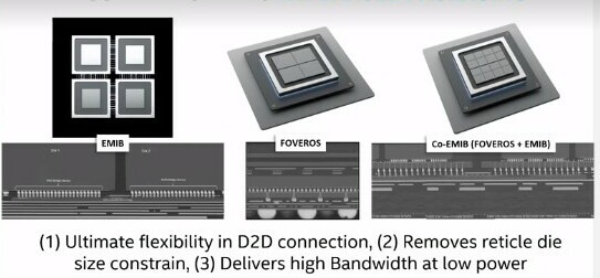
Intel’s current technology is shown below. EMIB is its Si bridge technology that is embedded in laminate substrates. It was introduced three years ago and is currently used in FPGA and CPU products. With EMIB there is no limit on reticle size. Foveros is its silicon interposer 3D technology. It has been commercial for 6 months in their Lakefield products. Co-EMIB is Intel’s architecture to connect EMIB and Foveros.
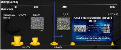
As packaging has become denser, we have had to move from laser fabricated vias to lithographically created vias as shown below.

The transition from solder-based interconnects to Cu-Cu based interconnect will be needed around 20-25µm. Hybrid bonding [see IFTLE 461] will come next with a transition around 10 µm. This will require advanced fab equipment with better precision and cleanliness.
Omnidirectional interconnect (ODI) involves the use of tall copper pillars to connect the chip directly to the organic package for signal integrity and power delivery.
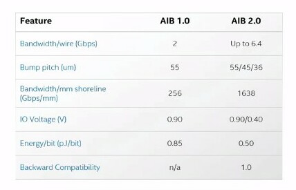
To enable the ecosystem, Sabi sees standardization similar to what took place in the board-level integration. It is necessary to connect different vendors’ products. Intel has introduced chiplet-to-chiplet interface known as Advanced Interface Bus or AIB. It was introduced 2 years ago in their FPGA products. AIB 2 has just been announced which promises higher bandwidth, tighter bump pitches, and lower power usage.
Sabi finished off his presentation touting the economic benefits of panel processing and the eventual need for photonics to replace copper, which they are currently working on under the DARPA program PIPES.
For all the latest in Advanced Packaging stay linked to IFTLE…………………………


