
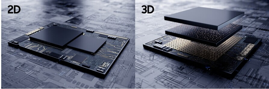
Samsung’s X-Cube
Samsung has announced that its advanced 3D integrated circuit (IC) packaging technology, dubbed “X-Cube,” is now available for advanced process nodes. The X stands for extended interconnect density and extended functionality
Samsung’s X-Cube silicon-proven design methodology and flow are available now for advanced nodes including 7nm and 5nm.
Samsung, currently the No. 2 player in the foundry industry, is reportedly using X-Cube technology to enable significant increases in speed and power efficiency for applications including 5G, artificial intelligence, high-performance computing, as well as mobile and wearable.
Samsung built a 7nm EUV test chip using this methodology by integrating an SRAM die on top of a logic die. The logic die is designed with through silicon via (TSV) pillars, which then connect to µ-bumps with only 30µm pitch, allowing the SRAM-die to be directly connected to the main die without intermediary mediums.
In 2014 Samsung disclosed its Exynos chips using “Widcon” technology [see IFTLE 305 “Where is Samsung Widecon??], stacking Wide I/O DRAM on top of logic through TSVs. But, this technology never reached commercialization for unknown reasons.
Samsung has stated that “…the evolution of the X-cube 3DIC solution will be the solution to beyond Moore’s Law.” The company released the video below.
Intel begins Hybrid Bonding
In IFTLE 457 we detailed how “Hybrid Bonding” was coming of age.
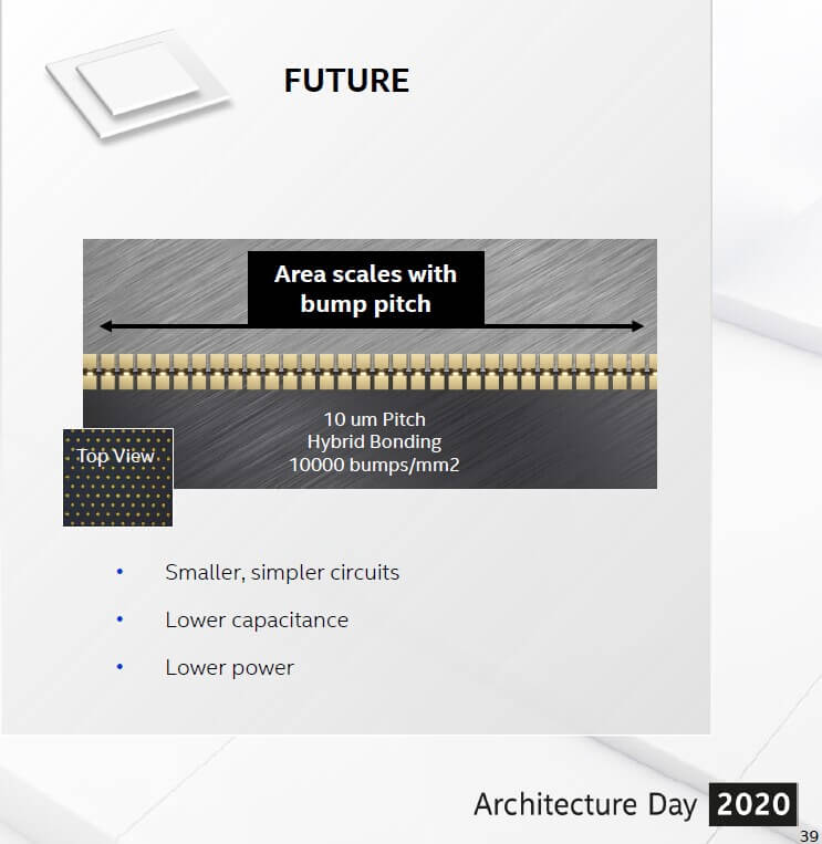
It looks like we can now add Intel to those jumping on the bandwagon. At Intel Architecture Day 2020 Intel’s Chief Architect, Raja Koduri, Intel fellows, and architects provided details on the progress Intel is making on what it calls its “6 pillars of technology innovation: process and packaging, architecture, memory, interconnects, security and software.”
The new packaging disclosure was that “…Hybrid bonding test chips were taped out in Q2, 2020. Hybrid bonding is an alternative to traditional “thermocompression” bonding used in most of today’s packaging technologies. This new technology enables very aggressive bump pitches of 10 microns and below, delivering much higher interconnect density and bandwidth, along with lower power.”
China busy Hiring TSMC engineers
Nikkei Asian Review reports that Two Chinese government-backed chip projects at QXIC and HSMC have together hired more than 100 experienced engineers and managers from TSMC over the last year.

The hirings are aimed at helping Beijing achieve its goal of fostering a domestic chip industry in order to cut China’s reliance on foreign suppliers like the USA.
Quanxin Integrated Circuit Manufacturing (QXIC), and Wuhan Hongxin Semiconductor Manufacturing (HSMC), founded in 2017 and 2019, respectively, employ more than 50 former TSMC employees each and are both led by ex-TSMC executives. The two projects are aiming to develop 14 nm and 12nm chip process technologies.
China’s top contract chipmaker, Semiconductor Manufacturing International Company (SMIC) recently announced capital spending for this year at $6.7B and announced it will build a $7.6 B joint-venture factory with “Beijing Economic-Technological Development Area”, a state-backed high-tech zone.
Nikkei reports that TSMC is very concerned that its trade secrets could be transferred to those emerging Chinese players and even asked chip-production equipment makers to sign a renewed pledge that they will not sell any customized tools for TSMC to the Chinese projects.
TSMC was reportedly uncomfortable when QXIC began operating a research and development base not far from the Taiwanese company’s most advanced 5nm plant in south Taiwan, one of the people familiar with the matter told Nikkei.
Nikkei estimates that Taiwan has in total lost more than 3000 IC engineers to China, Nikkei earlier reported.
For all the latest in Advanced Packaging stay linked to IFTLE……………………….


