

We’ve waited a long time for this, and now it’s here. There is a 3D megatrend happening in semiconductor manufacturing, as scaling alone does not meet the sophisticated computing needs of Industry 4.0 applications like blockchain, 5G, the internet of things (IoT), autonomous transportation, telemedicine, and more.
These emerging technologies call for more advanced technologies like artificial intelligence (AI), edge computing, deep learning, and machine learning, and even quantum computing. Bottom line: a smart, connected world needs more than just the faster processing and more data storage that finer nodes achieve. It needs full systems that incorporate sensing, logic, memory, power management, data transmission, and more. 3D integration is the key.
The 3D Megatrend Impacts Suppliers
This 3D megatrend is being realized in front-end semiconductor manufacturing in the form of 3D transistors (FinFETS) and memory (3D NAND, and DRAM) and 3D monolithic integration. In the backend, we are seeing the rapid commercialization of 2.5D and 3D architectures using fan-out wafer-level packaging (FOWLP), silicon interposers, through silicon vias (TSVs), and now chiplet integration.
High aspect ratio structures, new materials, and tighter geometries are putting the semiconductor suppliers through their paces to come up with process tools, materials, and inspection and test that meets the complex requirements of 3D. Added to that, the end-use applications require all these devices to be more reliable than ever, as they are not just targeted for smartphone apps, but those that impact our very lives.
But as always, the suppliers are rising to the challenge. Here are some recent exciting breakthroughs from Zeiss, Rudolph, CyberOptics, and EV Group, being showcased this week at SEMICON Taiwan, and earlier this summer at SEMICON West, that promise to further enable the 3D megatrend.
Process Control Solutions
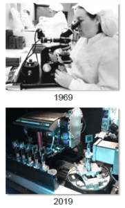
One of the greatest challenges of ensuring the reliability of 3D devices is measurement and inspection. I spoke with ZEISS’s Tom Gregorich, about how the company is leveraging its 3D tomography and X-ray capability during the development and prototype process to non-destructively measure and inspect bumps and connections buried deep inside 3D structures.
“Inspection in the back-end hasn’t changed much in the past 30 years. But with front-end scaling slowing down, and technologies like Foveros and Zen 2 (both chiplet approaches) being adopted, new support technologies are needed to enable them,” said Gregorich. “Our technology has been used in FA labs for nearly 10 years and allows engineers to non-destructively see deep inside packages. Now we have adapted that technology to 3D packaging measurement and inspection.”
Because 3D packages use a series of complex blind-and-buried processes to create the package structures, 3D measurement is not trivial, explained Gregorich. It is difficult to measure critical dimensions in 3D packages using conventional 2D inspection and measurement tools. Zeiss’s new Xradia 620 Versa RepScan includes ZEISS’s proven Versa 3D XRM capability to make it easy to do 3D measurement and inspection. The tool images and measures buried features like solder bumps and Cu pillars non-destructively with submicron resolution. It uses computed tomography to make virtual cross-sections in any plane and then extracts critical 3D information based on reconstructed 3D data sets. Engineers can then load the measurement data into statistical programs for further analysis.
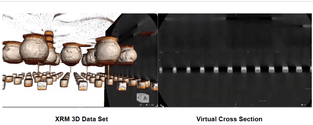
It also features a unique resolution-at-a-distance (RaaD) capability, which prevents sample images from being blurred or distorted as you move away from the source. RaaD maintains resolution regardless of its distance from the sample, allowing measurement of different sized parts.
The company introduces the tool this week at SEMICON Taiwan at Booth M0434. If you’re there, stop by. If not, you can learn more here.
Elsewhere in process control solutions that address the 3D megatrends, at SEMICON West I met with Tim Kryman, of Rudolph Technologies, who talked about how the company’s latest inspection tool for detecting die cracks. This is critical for automotive customers who require zero-defect packages. Wafer dicing and subsequent packaging process can cause the occurrence of die cracks of all types: edge, hairline, sidewall, and inner. Many of those cracks slip by conventional optical inspection processes, and while they may not impact final yields, can create device reliability issues downstream.
As prevention is the best way to eliminate cracks, Rudolph has developed a die crack detection process that combines hardware and software to improve control of the dicing process. In addition to enhanced optical detection and image processing, the tool ties in IR techniques to validate brightfield and darkfield capabilities, which allows for crack detection on both the front and backside of wafers. This article in Semiconductor Digest explains it best.
Rudolph’s forthcoming merger with Nanometrics will expand process control solutions from the front-end through to advanced packaging. This will also benefit the 3D megatrend happening across the complete semiconductor manufacturing value chain.
Stop by and visit the Rudolph Technologies team this week at SEMICON Taiwan, M0454 to learn more.
Also at SEMICON West, Dr. Subodh Kulkarni, President, and CEO, CyberOptics, gave me a demo of the company’s MRS sensor technology that is being integrated into backend inline inspection systems for optical inspection of bumps and Cu pillars used in 2.5D, 3D, and wafer-level packaging processes. Check out the video on Twitter.

Oops! Look what got stuck in the draft folder? Congrats to @CyberOpticsCorp for winning the #SEMICONWest Best of the West award for its MRS Sensor Technology, integrated into mid-end and advanced packaging inspection systems. Stop by booth L0310 at #SEMICONTaiwan @SEMIconex pic.twitter.com/q7z0XTqJXS
— 3D InCites (@3DInCites) September 16, 2019
MRS stands for multi reflection separation. It is a 3D non-contact optical sensing technology that uses digital light projectors to project patterns of light onto an object and measures x, y, and z dimensions to determine its height. MRS can do 2D and 3D inspection in the same pass, making it 2-3x faster than alternates.
“Customers in fabs or OSATS follow various steps making bumps or pillars. Before they flip the chip and glue it, they want to know the bumps and pillars are the right height and in the right location,” explained Kulkarni, “It is possible to rework or repair bumps and pillars using an additive process. If the device being build is a high-end GPU, you’ll want to take the time and fix the bump.”
CyberOptics will be showcasing its MRS 2D and 3D technology at SEMICON Taiwan. Stop by BOOTH L3019
3D Megatrend Lithography Processes
Advanced heterogeneous integration processes like high-density fan-out and chiplet integration are driving back-end lithography processes to meet finer geometry requirements. For example, resolutions for redistribution layers (RDL) and interposer are now in the range of 2µm and lower. Moreover, variation in both the substrate material and shape (round or panel, silicon, or organic) as well as die placement, requires more flexibility in patterning.
To address this, EV Group developed the world’s first mask-less exposure (MLE) technology for high-volume manufacturing (HVM). MLE eliminates the need for both masks and a stepper and instead uses steady-state writing technologies to make digital process files that are then used to create high-resolution photoresist patterns on any type of substrate. It supports all commercially available resist through a tightly integrated clustered write-head configuration and multi-wavelength high-power UV source.
With MLE it is possible to mix and match passives and active and active devices in the same pattern. And while steppers run into limitations as chips get bigger and go beyond reticle size, this is not the case with MLE. It can adapt dynamically and does not require stitching. It can also be used to address die shift by correcting the patterns on the fly. Learn more about MLE in this white paper.
MLE was launched this summer at SEMICON West. The company is offering demos at the company headquarters in Schärding, Austria. It will be incorporated into a new line of EVG tools.


