

Would it be flippant to say that the most pivotal event that impacted the commercialization of 3D integration technologies, may have been the commercialization of 2.5D interposer technologies? Arguably, 3D and silicon interposer are very different technologies, with a common denominator that happens to be the through silicon via (TSV). Until Xilinx announced its Virtix-7 2000T in or around 2011, skepticism was the other common denominator. 3D memory cubes were certainly in the ether at the time, but there was still much debate about the cost and commercial viability of TSV technologies.
Tasked as I was then with promoting 3D integration technologies, I was struggling to sell the larger picture of overall system performance benefit versus, say, the direct single-step cost adders such as metalizing a via or temporary handling of thin wafers or other such ‘inconvenient’ processes.
Ironically, yield was an often-used argument to rationalize that the cost of 3D would always be prohibitive. The notion of known-good-die (KGD) was considered difficult to measure, and how to accommodate yield multiplications related to stacking, remained a sticky question.
Then suddenly, along comes Xilinx with their silicon interposer, of which the TSV cost adder was paid for by none other than yield enhancement. Rather than building a single, very low-yielding large 28nm chip, Xilinx ‘simply’ (I use the word loosely) built smaller and thus better yielding 28nm chips and assembled them on an interposer. The system performance benefit ended up being financed by the very same yield that was supposed to be the problem. I say Xilinx, but of course, TSMC deserves their share of the credit too.
For me, this was a pivotal moment because suddenly the hypothesis that TSV technology would always be too costly to commercialize was clearly disproven. I must admit, I never anticipated that yield improvement would be the elusive initial justification for TSV integration costs – I was looking far and wide, and elsewhere.
So now, after publicly admitting, that I never saw that one coming … I’m expected to look into the same crystal ball and have you believe that I can see what’s coming next? Well, for what it’s worth …
The (very reliable?) crystal ball
Data generation, collection, analysis, storage and management (and dare I say abuse?) will continue to increase. Whether it’s due to the famous Internet of (every and any?) things (IoT), autonomous driving, high-performance computing or whatever, I think it’s fair to expect there will always be a demand for improved performance (specifically memory bandwidth) with reduced energy consumption and reduced cost. Traditionally, in terms of timing, the improved performance leads and the reduced cost follows. I say that because it conveniently allows me to ignore cost for what I’m about to forecast (experience tells me all I have to do is hang around until a future Xilinx-equivalent comes up with that solution!?).
Quantum computing is certainly a hot topic but let’s put it aside for the moment. As a rather pretentious professor once said to me; “there are two kinds of people – those who understand quantum mechanics, and those who don’t”.
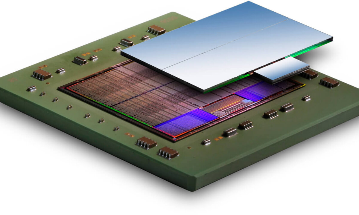
I must admit, I’m attracted to die-to-wafer hybrid (D2W) (a.k.a. direct) bonding. The wafer-to-wafer version (W2W) works very well. It’s my understanding that W2W hybrid bonding is more or less restricted to imager applications most likely due to the requirement that both dice must have the same size. D2W, however, removes the equal die-size requirement, which in theory could bring the performance benefits of hybrid bonding to almost any 3D system. And the performance benefits of hybrid bonding are not to be ignored: decreased interconnect pitch, shorter interconnects, faster communication, reduced loss, etc.
All of this sounds familiar because it’s basically the justification for any interconnect improvement ever proposed, including TSV’s back in 2011 – so it cannot be completely irrational to at least consider this approach (right?). D2W bonding could also enable, for the want of a better description, ‘partitioned-systems’ like the current interposer systems but with chiplets instead of chips, and active silicon interposers instead of passive silicon interposers.

Indeed, Intel has just announced its Foveros 3D integration scheme, which seeks to achieve competitive advantage by partitioning logic chips and stacking the resulting chiplets on top of each other. My organization, CEA, and others, such as DARPA, are also working on such initiatives (Figure 1).
Of course, D2W hybrid bonding will require some further development and collaboration before being sufficiently mature for industrial scale chiplet integration. Whatever performance the chiplet programs are achieving today, or planning to achieve, one could assume that the performance would be further increased with hybrid bonding. The Foveros technology seems to be relying on face-to-face, 36µm pitch µ-bump interconnects. However, with hybrid bonding, this pitch can be reduced to 5µm.
Many issues remain, not limited to dicing a perfect wafer surface (i.e. hybrid bonding requirement perfect!) in a way that the die surface is as perfect after dicing as it was before. Then picking and placing that perfect die surface on an equally perfect wafer surface with, by the way, very high alignment accuracy and high throughput. If Intel can live with the alignment accuracy versus throughput compromise of 36µm pitch interconnects, maybe we’re not actually that far from a 5µ accuracy/throughput compromise?
We know that D2W is possible in principle, and D2W electrical results have been demonstrated to be as good as W2W results. In any case, there is no fundamental reason that the electrical results should be different. We will need to develop a ‘clean’ dicing process along with some sort of auto-alignment system to fix throughput. Who knows, maybe the hybrid bonding with collective auto-alignment will end up being lower cost than, say, µ bumps + underfill or thermal-compression alternatives?
There you have it, my clear-as-mud crystal ball forecasts the introduction of D2W hybrid bonding at an industrial level, within 10 years …or thereabouts. ~ M. Scannell


