 You might recall that a few year’s back (October 2013, to be precise), 3D InCites’ regular blogger, Paul Werbaneth, had the opportunity to interview Dongkai Shangguan, then CEO of the National Center for Advanced Packaging (NCAP) in Wuxi, China, which he helped found along with nine investors. They talked about lots of timely topics: the importance of industry-wide collaboration to bring down the costs of 2.5D/3D packaging technologies; Asia as a hotbed for growth in advanced packaging, (thus the establishment of NCAP); how optimizing and customizing semiconductor processing equipment for advanced packaging applications will help equipment cost/performance improvements; and a number of other things. (You can refresh your memory here)
A year ago, upon completion of his term at NCAP, Shangguan joined STATS ChipPAC as chief marketing officer. I caught up with him in Las Vegas at ECTC 2016 for an update on where he sees the advanced packaging landscape changing in this time of mergers and acquisitions, growth in China, and the slowing of scaling per Moore’s Law.
The Back Story
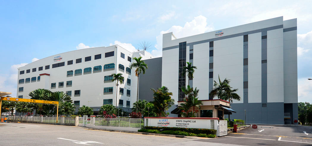
Shangguan joined STATS ChipPAC in the midst of its acquisition by Chinese semiconductor packaging conglomerate, JCET Group, comprising three companies each with its own management team. Jiangsu Changjiang Electronics Technology Co., Ltd. (JCET) is the largest outsourced semiconductor assembly and test service (OSAT) provider in China that mostly serves the Chinese market. Jiangyin Changdian Advanced Packaging Co., Ltd. (JCAP) provides wafer bump, probe and assembly, and STATS ChipPAC, headquartered in Singapore, rounds out the offering with a global manufacturing footprint and robust advanced packaging portfolio that includes wafer level packaging, flip chip and system-in-package (SiP) technology.
On The M&A Trends…
According to Research and Markets, 2015 was a record year for the total value of mergers and acquisition deals announced in the semiconductor industry, coming in at over $120B. The JCET acquisition of STATS ChipPAC was one such deal.
Consolidation is having an impact on the industry, and is a reflection of its maturity as a scaling economy, noted Shangguan. “Customers are getting bigger and demanding complete capabilities, services, and footprint. STATS ChipPAC and JCET are well positioned to sell bigger and larger,” he said. Together, he says the company will serve the semiconductor markets across North America, Europe, and Asia. “STATS ChipPAC has been strong in the North America and Europe,” he added. “With JCET’s strength in the Chinese market, we will be selling to customers all over the world and offering a broad portfolio from low-end, cost-sensitive products to high-end products.”
As a result of the acquisition, the JCET Group now has substantial manufacturing scale at various locations in China, including Jiangyin, Shanghai and Anhui, in addition to a sizeable manufacturing facility in Singapore which has significantly expanded its capacity recently, and a very large manufacturing operation in South Korea that is also currently going through a dramatic expansion. The Singapore factory focuses mainly on wafer level fan-in and fan-out technology, an area where there is growing demand in the market and the need for more capacity. The Korea operation, which was expanded and relocated to Incheon in 2014, is going through another considerable expansion to support growing demand for SiP solutions. “This is a new growth engine for us,” he said. “We continue to expand our SiP capabilities to support multiple market segments.”
On maturing FOWLP…
STATS ChipPAC was the earliest adopter of embedded wafer level ball grid array (eWLB), in production since 2009, and with 1B units shipped to date. Panel level processes, which will drive significantly better capital intensity and a lower unit cost for larger body sizes, are under development. “We are very strong and active in the fan-out space with mature processes. Yield is important and we have demonstrated very high yields with our fan-out process over the years. It takes time to build that through experience and expertise,” noted Shangguan.
On what’s driving the SiP and FOWLP markets…
“Packaging is a More than Moore solution; especially SiP,” noted Shangguan. “It’s an alternative path for system integration. SoC (system-on-chip) is one way, but SiP is a more flexible, cost-effective solution for system integration in many cases, particularly when heterogeneous technologies as involved.”
With the continued growth of the smartphone market and anticipated growth in sensor technologies for autonomous vehicles, the Internet of Things (IoT), wearable devices and more, they expect healthy growth for FOWLP and SiP. “SiP is everywhere,” he said. “There’s no doubt that the new advanced packaging landscape, including SiP and FOWLP, is changing the way semiconductor manufacturing does business. That’s why we have made the investment in capacity, floor space, and R&D.”


