In addition to attending the panel and plenary sessions at ECTC 2016, which took place May 31-June 3, 2016, I also spent a good deal of time talking to industry suppliers to get updates on their latest accomplishments that will impact the future of advanced semiconductor packaging, including interposer integration and 3D integration technologies.
Vincent Desmaris, Smoltek, told me all about the company’s molecular technology for growing nanostructures on substrates at temperatures below 390°C using chemical vapor deposition (CVD). “Temperature is critical so you don’t kill the component in the process,” explained Desmarais.
Although Smoltek’s processes were developed 10 years ago, achieving the low-temp aspect allows for nanostructure growth on an active device, making it possible to grow fine-pitch bumps directly on bond pads, or create on-chip capacitors.
Combined with interposer solutions, this also enables an energy storage solution that can be integrated with a sensor so it doesn’t need to rely on an external battery. This seems like a real breakthrough for the wearable device market.
Desmaris admitted that while CVD is a costly process, he thinks that front-end processes are beginning to be more accepted in the back-end. He’s provided some technical information that you can find here in the 3D InCites Knowledge Portal.
You might recall that at the 2014 IMAPS Device Packaging Conference, Kim Pollard, Dynaloy, presented results of ongoing feasibility studies for post-Bosch process residue removal using a solution with an improved environmental health and safety (EHS) profile. The goal was to develop a one-step process that removes both the photoresist polymer and the fluorine residue that remains on the via sidewall post-etch. The current method is a two-step process, in which the polymer is first removed using an oxygen plasma ash process. Then a wet process is used to remove the fluorine residue. Eliminating the ash step would provide considerable cost savings.
All went well in the first phase of the study done in Dynaloy’s labs on sample coupons, in which pre-screening showed fluorine was present, and subsequently removed with the new chemistry. However, in the second phase, which was performed using Dynaloy’s chemistry on full wafers in an SSEC wet wafer processing system, the wafers did not show any residual fluorine, so even though the wafers were clean at the end, conclusive data could not be provided. I wrote about it here.
Now, two years later, that conclusive data is available, thanks to the ongoing efforts of Pollard and Laura Mauer, CTO of Veeco Precision Surface Processing (formerly SSEC). The team compared the performance of Veeco’s wet process sequence in its WaferStorm platform with a more traditional process using oxygen ash, SC1 and HF clean. During the interactive poster session, Mauer reported that the combined chemistry and process not only cleans as well as the traditional approach, it eliminates the need for the ash step, reducing TSV RIE process time by 33%. This time, auger electron spectroscopy did show polymer and photoresist residue before cleaning. Electrical and physical analysis showed that the Veeco wet clean process removed both. Download the poster here.
At the KLA-Tencor booth, Pieter Vandewalle showed me several important developments with the ICOS T830 Component Inspector that targets the latest requirements for optical inspection of system-in-package (SiP) modules. First, he said as finer features are driving the industry to replace EMI shielding cap with metal coating spray, it’s critical to find exposed Cu defects in the shield coating to ensure the quality of the shield. This requires full-color inspection, which has been added to the tool. Inspection is performed right after sputtering to monitor the process and again after the functional test, explained Vandewalle. Additionally, he said there is a device cleaning feature consisting of a brushing system to remove burrs on the bottom of the EMI shield. The tool was selected for TSMC’s InFO process.
The next critical area for inspection is ball height for fan-out wafer level packages (FOWLP) in a package-on-package (PoP) configuration. The height of the total PoP stack is critical for smartphone manufacturers, and there is a tight tolerance on package height. For this, KLA-Tencor has added an entirely new module with a 3D measurement technique that measures with 5µm accuracy.
The last area Vandewalle touched on was the impact smaller nodes (14nm and below) is having on fan-in wafer level packaging. The use of low-k dielectrics is resulting in delamination and sidewall cracks because of the brittleness. To address this from an inspection perspective, KLA-Tencor will be introducing fast infrared inspections. Details were not available at this time.

 In addition to these in-depth briefings, from a stroll through the technology corner I learned that:
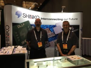
Shinko has developed an organic interposer for 2.5D integration that reaches 2/2µm line and space feature sizes. Did you know that Shinko is not just a substrate supplier? It is a full-blown outsourced semiconductor assembly and test service (OSAT) provider (albeit a small one.)
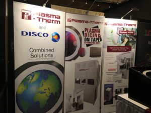
Disco is partnering with Plasmatherm to develop plasma dicing technology.
Samtec, another packaging house that specializes in substrate selection, signal integrity, and design, has acquired nMode Solutions and its subsidiary, Triton Microtechnologies, Inc. If you recall, Triton has made a name for itself in the past few years for the development of glass interposer and through glass via (TGV) processes – something Samtec sees as an enhancement of its IC packaging capabilities that currently include wire bond, die attach, flip chip and underfill. This is their foray into the 2.5D world.
I’m sure this is just the tip of the proverbial iceberg of the latest innovations. With SEMICON West right around the corner, I’m looking forward to learning more from suppliers and will bring you all the latest on 3D InCites. Stay tuned! ~ FvT


