

 Some technologies take forever to cross the chasm into successful commercialization. Or they never do, and end up together with Wile E. Coyote at the bottom of the canyon.
My take today is that heterogeneous integration is showing signs of a successful chasm leap. Heterogeneous integration is going to be the Roadrunner.
Therefore, we intend, at 3D InCites, to cover the topic of heterogeneous integration in a new blog, 3D+: Inspired by Heterogeneous Integration, which will be a regular feature running alongside all the other great content you’ve been reading ever since 3D InCites went live with its mission of “Stirring Up Interest in 3D Integration.”
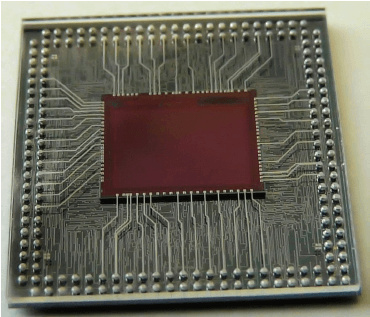
![]() Heterogeneous Integration is going to be the next important commercial story in 3D Integration, and 3D+ will be on the scene reporting and offering insights on the latest developments from Academia (yes, from you James Lu, at RPI; and from you, Koyanagi-sensei at Tohoku University; and from you, Rob Andosca / Microgen; and you, Janusz Bryzek, the Trillion Sensor Man at Fairchild); and from The Street (that’s you, Robert Maire, at Semiconductor Advisors LLC – what do you think about the MicroChips – SiTime acquisition?).
Heterogeneous Integration is going to be the next important commercial story in 3D Integration, and 3D+ will be on the scene reporting and offering insights on the latest developments from Academia (yes, from you James Lu, at RPI; and from you, Koyanagi-sensei at Tohoku University; and from you, Rob Andosca / Microgen; and you, Janusz Bryzek, the Trillion Sensor Man at Fairchild); and from The Street (that’s you, Robert Maire, at Semiconductor Advisors LLC – what do you think about the MicroChips – SiTime acquisition?).
I am on record, almost five years ago, for having written: “I think heterogeneous integration is the way 3D-IC manufacturing techniques are going to launch into the commercial mainstream … I’ve said this before, but when you step outside US-centric thinking and look to see what Japan and the EU are doing with 3D IC, it’s all about adding functional value, or introducing novel products, via heterogeneous integration. Don’t know why we don’t hear more about heterointegration from the home team sluggers.”
Why would heterogeneous integration have been on my radar in 2009?
Because my radar picked it up even earlier than that. A little more than ten years ago, I co-authored the paper “Plasma Etching of Thick BCB Polymer Films for Flip Chip Bonding of Hybrid Compound Semiconductor-Silicon Devices,” for GaAs MANTECH 2004: “Integration of passive electronic components directly over silicon substrates and packaging of active compound semiconductor devices along with silicon CMOS device via flip chip bonding are two technologies that have seen increased popularity over the last several years for high speed / high frequency applications in the wireless and fiberoptical communication industries. This space-efficient and reliable hybrid integration scheme offers significant advantages in device performance as well as in manufacturing cost.”
I was interested (inspired), ten years ago, in methods for combining separate parts or elements (GaAs and silicon devices, in this example) into a unified whole (integration), the unified whole consisting of elements that weren’t of the same kind or nature (heterogeneous).
I think my personal heterogeneous integration history goes back further than that, but the Google trail runs cold …

 Was I early in my enthusiasm for heterogeneous integration as a commercially important branch of semiconductor processing technology? Not nearly as early as many of the other enthusiasts and practitioners in the field, but early enough so that the work was mostly pre-commercial, looking to cross the chasm, as so many other advanced technologies have been over the years my colleagues and I in the plasma etch and PVD world contributed to them.
(From my Twitter profile: “Keen on Packaging, 3D-IC, MEMS, and III-V; have seen a few technologies succeed, and a few fail to ever cross the chasm. Prefer the former to the latter.” Follow me @PFWerbaneth.)
There’s an Internet of Things angle too to follow here – the real IoT won’t be getting much off the ground without (cheap) heterogeneous integration.
Françoise von Trapp is already on the heterointegration case, prescient once again; from 3D InCites, 16 January 2014, we have: “Europe in 3D: The Brains behind e-BRAINS” “After so many years covering 3D technologies, I love finding a new angle to write about. Yesterday’s visit to Fraunhofer EMFT in Munich provided just that. Instead of focusing on 3D IC processes, we talked about 3D systems integration and the e-BRAINS project. And rather than discussing the well-worn topic of mobile applications, we talked about other markets that stand to benefit from 3D heterogeneous integration, such as medical devices and industrial applications.” (That’s you, Peter Ramm, department head, heterogeneous system integration at Fraunhofer EMFT.)
 And I’ll be at the MEMS Executive Congress US 2014 in Scottsdale, AZ this week, getting the 3D+ ball rolling, running alongside the roadrunners in heterogeneous integration as they zip forward, leaving chasm-bound coyotes in their dust. From Pittsburgh, PA, thanks for reading. ~ PFW


