
The semiconductor industry hasn’t adopted 3D ICs as quickly as many in the industry expected. There are some barriers that perhaps have kept the cost/benefit analysis stuck in the ‘scaling’ camp rather than moving it to the ‘3D’ camp. However, many companies are preparing for the move to 2.5D and 3D in the future. From a DFT perspective, the barriers are actually quite low; designers have methodologies now to stack their memory on logic, including the ability to test stacked ICs. The test strategy for 3D ICs has two goals: to support high yields and to establish plug-and-play DFT and test patterns. From our DFT perspective, there are a few mistakes you can avoid when thinking about designing, or beginning the design, of 3D ICs.
Don’t limit your test flexibility.
Will you try to use separate interfaces for die, stack, and partial stack test? Is there a different test access point (TAP) on each die? How will you access them after packaging? You can create a plug-and-play test architecture on each IC that allows die, stack, and partial stack level tests to use the same test interface, and to retarget die-level tests directly to the selected die within the 3D stack.
We use an IEEE 1149.1 (JTAG) compliant TAP as the interface at every die and IEEE P1687 (IJTAG) networks and definitions for test access. In a 3D package, only the TAP on the bottom die appears as the test interface to the outside world, in particular to the ATE. The same TAP structure is used on all die, and they accept special instructions to enable the next-level TAP in the stack. From outside of the 3D package, for board-level test for example, the 3D package appears to contain only the one TAP from the bottom die (Figure 1).
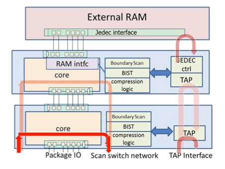
You can also use IEEE P1687 (IJTAG) to model the TAP, the test access network, and test instruments contained within the die. IJTAG is based on and integrates the IEEE 1149.1 and IEEE 1500 standards, but expands beyond their individual possibilities. It provides a powerful means for the test strategy to adjust to and adopt future test features.
Don’t neglect pre-packaged die test quality.
Because silicon area is a key factor in determining yield, 3D ICs can actually improve yield. The larger the die, the more likely it contains a fabrication defect. With 3D ICs, you can design the functionality on multiple, smaller, better yielding die that are individually tested before being packaged together.
So, to avoid having to throw away packaged 3D stacks due to one defective die in the stack, thorough die-level test with memory built-in self test (BIST), automatic test pattern generation (ATPG), logic BIST, and die I/O test is key. An important feature of memory BIST is to be “soft-programmable” so algorithms can be selected and/or programmed as needed based on what is learned during production. For logic test, you can combine ATPG plus logic BIST that uses common test logic for both functions. ATPG provides an infrastructure for standard stuck-at, transition, and path delay tests, as well as newer high-quality tests such as timing-aware, cell-aware, and other specialized types of test. The logic BIST part allows for in-system test that is particularly important to ICs for automotive or medical applications.
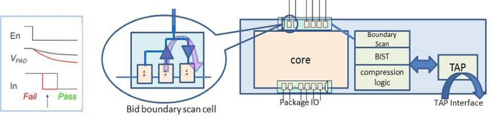
For die I/O test based on IEEE 1149.1 boundary scan, bidirectional boundary scan cells are located at every I/O to support a contactless test technique known as “I/O wrap.” Figure 2 shows an example of how I/O wrap test works. Using boundary scan logic like this enables test at the die-level of the partially packaged device, and of the interconnect between packaged dies. The TAP and boundary scan logic performs an infrastructure test and a wrap test on each boundary scan cell I/O. A contactless leakage test is also included; the die I/O can thus be tested for excess leakage during wafer and other tests through contact with only the TAP signals.

Don’t make unnecessary tests.
There is no reason to make different tests for the die and 3D package. Use hierarchical DFT methods instead. This lets you complete most of the DFT insertion and ATPG on individual blocks/chips as they are ready, and then use software to map the core-level ATPG and BIST patterns to the top-level design and retarget the test patterns automatically. The DFT logic and patterns for any die can be retargeted to any package in which the die is used. Thus, if the die were used in multiple packages, then only one DFT insertion and ATPG effort would be necessary, which would then be retargeted to all the platforms where it is used. While 3D IC test standards, test requirements, and the types of external memories being used are still evolving, you can get it done with technology available today. ~ R. Press
About the Blogger
Ron Press is the technical marketing director of the Silicon Test Solutions products at Mentor Graphics. He has published dozens of papers in the field of test, is a member of the International Test Conference (ITC) Steering Committee, and is a Golden Core member of the IEEE Computer Society, and a Senior Member of IEEE. Press has patents on reduced-pin-count testing and glitch-free clock switching.


