

The good news: While forecasted dates for 3D IC volume manufacturing continues to be pushed out, clearly foundries and OSATS are gearing up to be ready when it does.
The bad news: Forecasted dates for volume manufacturing of 3D ICs keep being pushed out. Or do they?
Rick Merritt, EE Times, posted a detailed news analysis piece today titled 3-D IC stacks pushed back to 2015, that talks about many of the concerns that still remain, and includes interviews with Dave McCann of GlobalFoundries, and Herb Reiter of eda2asic, and delves deeply in to such areas as costs and yields, and 2.5D and 3D tests.
While I agree with the majority of Merritt’s analysis, I disagree with his opening statement that “plans to make 3-D chip stacks for next generation smartphones have been pushed out to 2015 or later.” The operative phrase here is “for next-generation smartphones” and in this case I would say “pushed out” is inaccurate – at least as a current news item.
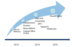
Over a year ago at the BITS Workshop 2012, Jim Feldhan of SEMICO Research shared this applications roadmap, where smartphones appear at the tail end in 2016 (Figure 1).
The reality is that for some time, industry experts have been saying HVM for smartphones won’t happen until the cost comes down and there are no less expensive alternatives to achieve the required performance. But there are plenty of high-end computing applications that will get the ball rolling and as production and yields go up, prices will come down. (See yesterday’s blog on Wright’s Law.) We have to walk before we can run, people.
In the mean time, there have been other promising announcements that indicate the industry is gearing up to handle HVM of both 2.5D and 3D IC technologies:
United Test and Assembly Center (UTAC) has thrown its hat into the ring to “join the scarce list of suppliers in offering fine-pitch 2.5D TSI packaging solutions” by entering into a collaboration with A*STAR’s Institute of Microelectronics (IME) to develop a HVM platform for 2.5D silicon interposers.

According to the announcement, IME will contribute its R&D expertise in design and advanced packaging to address electrical, thermal, thermo-mechanical and reliability requirements for applications including mobile devices such as tablets and smart phones. The optimized 2.5D TSI technology from this collaboration will be transferred to UTAC for high volume manufacturing, with the intention of significantly shortening UTAC’s time-to-market.
GlobalFoundries also announced a major milestone in its 3D IC strategy. The company demonstrated its first functional 20nm silicon wafers with integrated Through-Silicon Vias (TSVs). Migrating TSV technologies from 28nm to 20nm is a challenge, which GF engineers have overcome thanks to the development of a proprietary contact protection scheme that enables TSV integration with minimal disruption to its 20nm-LPM platform technology. David McCann, VP of packaging R&D at GlobalFoundries sees this as sign that 3D ICs will soon be a reality. The next step, he says, is to leverage these capabilities in collaboration with GF’s OSAT partners to to assemble and qualify 3D test vehicles.
And finally, in late March, both EV Group and SUSS MicroTec announced significant tool orders and installations for their respective wafer bonding clusters. EV Group reportedly installed a fully automated 300mm system in a leading Chinese semiconductor foundry. The system will be used for 3D IC integration and advanced packaging. SUSS MicroTec’s order is for its latest generation of high volume manufacturing temporary bond clusters that will be configured to temporarily bond and debond 300mm wafers for 3D integration processes in logic and memory applications using the TMAT (Thin Materials) process and adhesive materials. While neither company is at liberty to divulge the name of its customer, this clear indication of major players adding HVM capacity suggests a note of confidence for commercialization of 3D ICs.
So lets circle back to the good news and bad news. In reality, the implied bad news is really non-news, because the application roadmap for smartphones has remained stable for more than a year as reality set in. And back in early December at the 3D ASIP Conference, Dave McCann gave a keynote speech during which he said that GlobalFoundries will be ready for commercialization when customers are: 2.5D interposers by the end of 2013 and full 3D IC by 2015.
While we all wish 3D ICs were moving faster towards HVM, at least they’re moving in the right direction. ~ F.v.T.


