
Oh yes, where was I before the holidays took over and hijacked my life for two weeks? I’ll bet you thought I was done reporting on 3D ASIP, but wait – there’s more!
Point/Counterpoint on Thin Wafer Handling
I already reported on Wilfried Bair’s (Suss MicroTec’s perspective on temporary/ debond bonding here. EV Group has also been working to overcome the thin wafer handling hurdles that have plagued the progress of 3D IC adoption. In his presentation, Thorsten Matthias, director of business development, said that the “name of the game” is stress and yield management, which requires chip-package co-engineering. He says if you can control the stress of the wafer and therefore maintain flatness, there are more adhesives to choose from and a larger process window.
Matthias also explained the concept of “smart process integration”, a process flow EVG has developed that is optimized for manufacturing and minimizes processes as a way to manage cost of ownership (CoO). For example, using Cu-Cu fusion wafer bonding to form a pre-bond at room temperature followed by a batch anneal process results in 20 bonds per hour because you don’t have the high temperature step, and allows for the quality of the bond to be inspected in situ so that it can be separated and rebonded if necessary. Matthias says this method results in 100% yield for the bonding process.
Citing “lessons learned” from image sensor manufacturing technology, he talked about fine pitch interconnects, bumpless bonding, wafer-to-wafer integration for memory processes, and thin die stacks without thin wafer handling for interposer applications.
Cost Models for Interposers
It’s official. Applied Materials’ Sesh Ramaswami is a man after my own heart. When he opened his presentation with the comment “we need to remove the word “packaging” and focus on interconnects. It’s a psychological problem.“ I almost jump up and shout “YES!” Because that’s what I’ve been saying for some time! (Read Interconnectology: A Call To Arms here ) In fact, we’ve got a panel discussion coming up in March at the BiTS Workshop to talk about this. But I digress. Ramaswami talked about foundry readiness for via creation, and said increased attention is being paid to the process window, technology extendibility, and manufacturing cost as end-product companies focus on transitioning from technology qualification to manufacturing. “Now that (via) processes are ready, the goal is to tweak them and work with them to discover how to lower cost. “ he said.
Ramaswami presented the day after Lionel Cadix, packaging analyst of Yole Développement, presented a cost model for silicon interposers based on Xilinx Virtex 7. The cost model was based on an assumption of 98% yield, and calculated interposer manufacturing wafer costs at $683, sold at a price of $1707; broken down to a manufacturing cost per interposer die of $12 and interposer price part of $30.
The jury is still out on the accuracy of the cost model. While Phil Garrou told me in his opinion, it’s “pretty close” (read his blog post, Lifting the Veil on Silicon Interposer Pricing here), several attendees questioned the assumptions used and the model itself. Cadix admitted that the company is still working on perfecting the model. He also noted that most of the budget is linked to TSV cost, and that with packaging assembly cost added in, we’re looking at a price point of $53.47 per package.
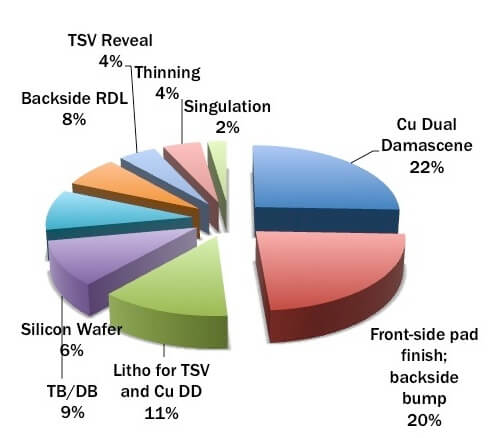
Ramaswami took this opportunity to provide further cost analysis of the TSV interposer wafer cost. He said he based his analysis on “assumptions used by presenters” and of the $500-650/wafer, determined the lion’s share of the cost is divided between the 3ML Cu damascene layer (22%) and front-side pad finish and backside bump, based on 10×100µm TSV mid process. (20%). The rest of his breakdown is as follows:
 Ramaswami points to the backside bump process as a place to focus on for cost reduction, as damascene processes have been optimized and there isn’t much room for improvement. He also note that market adoption will help focus and accelerate cost improvement programs as products come on line.
Test: A Necessary Evil or A Value Creator?
Offering a new perspective, imec’s Erik Jan Marinissen (aka King of 3D Test) presented COSTAR: A Cost Model of 3D SiCs to demonstrate the added value pre, mid, and post bond testing can bring to 3D IC manufacturing by helping to understand defects and improve yields. While it’s true that initially test adds cost, which should be minimized, ultimately Marinissen explained that up-stream testing can reduce down-stream costs.

Unlike 2D test flows, 3D stacks offer many potential test moments. Therefore there is no one-size-fits-all test flow, but rather many different options based on different parameters. Therefore cost-modeling is critical to optimize the tradeoffs. Through demonstration of 3 case studies: pre-bond interposer, pre-bond microbump probing, and mid-bond test, Marinissen deduced that typically, all three test points do ultimately pay-off, as long as certain parameters are adhered to. Specifically his work surmised:
- Pre-bond interposer testing results in a reduction of total stack costs by preventing use of known-bad components in the stacks.
- Probing on micro-bumps is cheaper than testing through dedicated extra probe pads.
- For mid-bond testing, the order of stacking is important; its best to stack them in order of increasing cost.
The Next Big Tech Thing
While most of the presentations focused on offering solutions to remaining pain points so that 3D ICs can become commercialized, there’s already talk of what’s coming next to improve performance benefits. In a word: it’s photonics. Carl Engblom, of ST Ericsson planted the initial seed during his keynote address on the needs of wireless networking. He said there’s a need for heterogeneous integration of logic and memory to deal with coming challenges, but that it takes a 3X performance improvement to justify hardware upgrade. In the short-term, he says 2.5D interposer technology is “good enough” but what’s really needed is a “technology leap for interconnect technologies” and that silicon photonics offers a viable solution that solves existing Cu interconnect limitations of bandwidth, delay and energy efficiency. He talked about a unified approach across the electronics ecosystem to develop Optical Short Reach Interconnects (OSRI), which are essentially an active optical interposer.
However silicon photonics have issues, such as what Jan Vardaman called the ‘bending the light problem” – or how to launch light straight into PCBS – which has thus far been a show-stopper. While Engblom wasn’t at liberty to disclose work being done to solve that, he seemed quite confident in declaring that OSRIs will be available in 2014 and common in 2016-2017.
Photonics is also firmly on Tezzaron Semiconductor’s radar, according to Bob Patti. “We can get tons of bandwidth on the module, but we can’t get it off the module (using Cu wire) ,” he explained, “Photonics is the answer.”
Surya Bhattacharya of the Institute of Microelectronics (IME) explained how the research center’s work with through silicon interposer (TSI) incorporates Si photonics into the 2.5D heterogeneous design and integration platform. It is considered to be a ‘medium term’ solution integrated with a passive TSI and a ‘long term’ solution is to integrated it with an active TSI. Cu types of I/O on TSI are limited, explained Bhattacharya, and integrating Si photonics on TSI can enhance system performance by reducing I/O power and Increasing bandwidth. And although there are critical technology and design challenges, the building blocks exist, and integration challenges should be solvable.
And I think that’s it on 3D ASIP until next year! I think… F.v.T.


