Fogale Nanotech has been on my radar with its 3D TSV metrology solutions ever since I noticed their booth last summer at SEMICON West. Sometimes it takes an occasion such as a pre-arranged interview at the European 3D TSV Summit for a connection to finally take place. I was happy to have such a moment last week, and sat down with Gilles Fresquet, to learn more about Fogale’s metrology solutions for 3D IC TSV integration process control.
Like many French hi-tech start-ups, the company, headquartered in Nimes, France, is a spinout of French national laboratory CEA and Onera. Fresquet explained that initially, the TSV optical metrology began with MEMS applications, and has now been adapted to perform 3D IC process control. He talked about the tool’s core technology, which is an optical head that combines different technologies including IR sensor, white light/Infrared microscopy, multi-wavelength bandwidth IR interferometery, and chromatic confocal capable of monitoring all specific processes related to 3D IC applications.
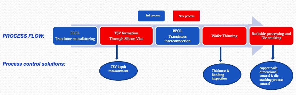
What differentiates this technology from others in the field is the ability to perform all these functions in one step in the same optical path, explained Fresquet. Target applications in the process flow include backside processing and RST measurement (measuring remaining silicon thickness prior to thinning to find the depth of the TSV); Cu nail height and coplanarity; and die stacking. So for example, in the case of the temporary bond/debond process, in one pass you can measure the total thickness variation (TTV) of the whole stack to determine bow/warpage, while taking an IR image of the interface between the two wafers to check for voids or delamination.
The tool is “well adapted for pilot lines,” said Fresquet, because it offers a versatile solution by allowing for mode selection based on the process step. Additionally, he said the the ability to customize it by adding or removing sensors means its easily upgradable and flexible. While the optical head is currently part of a stand-alone tool, Fresquet said it would be possible to adapt it for in-situ process control inside a wafer bonder.
Collaboration with both customers and academic partners has played a large part in the development process along the way, notes Fresquet. For example, through troubleshooting with US partner, Nanometrics, they were able to reach a higher level of resolution. The company has been involved with collaboration programs worldwide including IEF Paris, ITRI, Leti, imec, and SEMATECH.

Plans are now underway for a high-volume manufacturing (HVM) tool for 200mm and 300mm wafers that can detect a void in one minute. Fresquet claims that its large field-of-view objective will be able to achieve the same resolution of acoustic microscopy – <50µm resolution –while simultaneously measuring TTV. I expect we’ll be hearing more from Fogale Nanotech in the years to come. ~ F.v.T.