
In the world of semiconductors and microelectronics, a trend to vertically stack integrated circuits (ICs) or circuitry has emerged as a viable solution for meeting electronic device requirements such as higher performance, increased functionality, lower power consumption, and a smaller footprint. The various methods and processes used to achieve this are called 3D integration technologies.
In general, 3D integration is a broad term that includes such technologies as 3D wafer-level packaging; 2.5D and 3D interposer-based integration; 3D stacked ICs (3D-SICs), monolithic 3D ICs; 3D heterogeneous integration; and 3D systems integration.
What is the difference between 3D Packaging, 2.5D interposers, and 3D ICs?
3D packaging refers to 3D integration schemes that rely on traditional methods of interconnect at the package level such as wire bonding and flip chip to achieve vertical stacks. Examples of 3D packages include package-on-package (PoP) where individual die are packaged, and the packages are stacked and interconnected with wire bonds or flip chip processes; and 3D wafer-level packaging (3D WLP) that uses redistribution layers (RDL) and bumping processes to form interconnects.
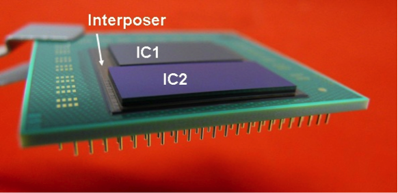
2.5D interposer is a configuration where dies are mounted side-by-side on a silicon, glass, or organic interposer using through silicon vias (TSVs) through the interposer. (When glass or organic laminate is used as the interposer substrate, the vias are called through glass vias (TGV) and through substrate via (TSV) respectively.) Communication between the dies takes place via circuitry fabricated on the interposer.
CMOS image sensors (CIS) have TSVs as backside vias to form interconnects, eliminate wire bonds, and allow for reduced form factor and higher-density interconnects. In all types of 3D packaging, chips in the package communicate using off-chip signaling, much as if they were mounted in separate package on a normal circuit board.
3D ICs can be divided into 3D Stacked ICs (3D-SICs), which refers to stacking IC chips and interconnecting them with TSVs; and true 3D ICs, which use fab processes to stack multiple device layers on a single chip, which may or may not use very-fine-pitch TSVs to form the interconnect.
What are Through Silicon Vias?
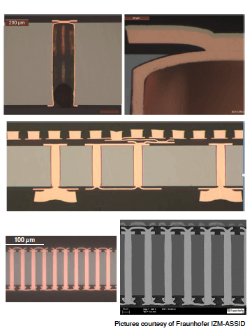 Through silicon vias (TSVs) are holes created in a silicon wafer using an etch process. Interconnects are formed by filling TSVs with a conductive material, such as copper, tungsten, or polysilicon (figure 2). The main advantage of TSV interconnects is the shortened path for the signal to travel from one chip to the next, or one layer of circuitry to the next. This allows for reduced power, and the ability to increase interconnect density, thereby increasing functionality and performance. TSVs are not 3D ICs all by themselves. Rather, they are the building blocks that enable 3D ICs. Backside vias are also used in other devices such as image sensors, microelectromechanical systems (MEMS) and compound semiconductors.
What is meant by monolithic 3D ICs?
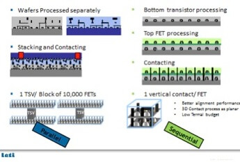 Rather than stacking wafers or die to create 3D ICs,monolithic 3D ICs begin with a base wafer onto which additional layers of crystallized silicon, metalized layers and active as well as passive circuitry are added using traditional fab equipment (Figure 2). The vertical interconnects are formed between layers rather than chips, using vias in the nanometer rather than micron range; as is the case with TSVs. There are several different approaches being developed, targeting mainly memory applications. Monolithic 3D is also sometimes called Sequential 3D.
What is 3D memory?
 There are a number of approaches being developed to stack memory vertically for both non-volatile (NAND Flash) and volatile (DRAM) memory devices. DRAM approaches include high-bandwidth memory (HBM), Micron’s Hybrid Memory Cube, and Tezzaron’s disintegrated RAM (DiRAM). All of these are based on 3D ICs using TSVs (Figure 3). Samsung, Toshiba and a number of other companies are developing 3D NAND Flash, based on monolithic 3D approaches.
What are the benefits of 2.5D interposer technologies?
2.5D technology was first developed to be a bridge technology to 3D ICs, and has grown to be a package platform that is expected to co-exist alongside 3D ICs. Unlike in 3D-ICs, only the interposer, and not the dies themselves, needs TSVs to connect active die with package substrates. This allows for the use of existing die designs.
What are the main technology drivers for 3D integration?
The increased costs of lithography steps and wafer processing in general at the next-generation silicon nodes are driving the industry to find alternatives to improve the performance and functionality of our electronic devices, lower the cost. Additionally, the need to integrate disparate technologies (logic, memory, RF, sensors, etc) in small form factors is driving the industry to 3D integration as a solution.
What are the market drivers for 3D integration?
The market drivers for 3D integration begin with high-end computing, servers and data centers, military and aerospace, and medical devices, because they have the greatest need and can bear the cost of current 3D integration technologies. Tablets, smartphones and gaming devices are also driving the technology.
What are the challenges being faced by 3D ICs?
While many claim there are no remaining technology challenges—and that those that are left can be easily engineered out—certain process steps still need better solutions, namely, design tools for planning, implementing and verifying 2.5D and 3D ICs, thin wafer handling, thermal management, and test. The main challenge is unit cost at the current, low volumes and implementation risk, due to a slowly maturing ecosystem. Efforts are underway to reduce process costs and streamline industry-wide cooperation. Yield improvements will enable cost reduction. However, many 3D experts believe that implementing 3D ICs will reduce system costs considerably, and that the remaining challenge is educating the system-level engineers about the benefits of designing 3D ICs into their systems.
What forms of 3D integration are already in production?
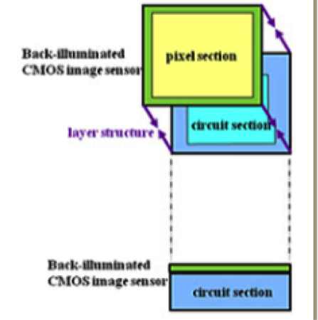
CMOS Image Sensors (CIS) were the first devices to implement via-last backside vias at high volumes. CIS with backside illumination (BSI) is now in production, and as the CIS is stacked on top of the IC, it is a 3D IC device (Figure 2). Xilinx introduced 2.5D interposer designs in 2011 with their Virtex-7 family of all programmable FPGAs.
Tezzaron has delivered DiRAMs in lower volumes for the past few years.
In late 2014, Micron and Samsung are expected to begin production of the hybrid memory cube (HMC), which is a 3D DRAM stack on top of a logic device. SK Hynix will offer HMC and High Bandwidth Memory (HBM) at the same time. The high-volume production of these 3D integrated memory devices is expected for 2014 /15 and will continue with logic stacks and heterogeneous devices over the next few years.