
BeSang Inc, a fabless semiconductor company in Beaverton, OR, has been on my 3D IC radar since 2008, when I first edited a 3D technology cover feature in Advanced Packaging Magazine, written by George C. Riley, that included a status report on BeSang’s TRUE 3D ICs™, which had just been demonstrated. What I didn’t understand then, that I know now, was that this was an example of what we today call “monolithic 3D ICs” vs 3D IC stacking using through silicon via (TSV) technologies.
After a year or so of quiet, BeSang Inc, has recently reappeared in the news with a fairly substantial announcement of a license to Hynix for its “TRUE 3D IC™” process, which Hynix will reportedly use across a broad range of products, among them, DRAM. Up until now, all the news surrounding BeSang was about its technology accomplishments, patents, awards and trademarks (They’ve actually trademarked the TRUE 3D IC moniker). This announcement was worth a sit-up-and-take notice as it raises some questions about the impact this will have on the commercialization of TSV-based 3D DRAM technology such as the Hybrid Memory Cube (HMC), High Bandwidth Memory (HBM) and Tezzaron’s disintegrated RAM (DiRAM).
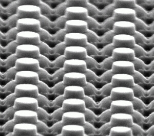
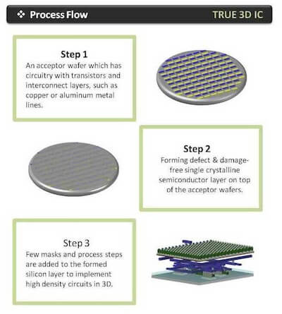
Rather than stacking die and interconnecting them with TSVs (the 3D IC definition we are most familiar with), BeSang’s technology is a low-temp, “single-chip 3D IC solution with unrestricted 3D interconnects” that uses traditional vias to build multilayer 3D ICs. This article by R. Colin Johnson, for EE Times. gives a fairly detailed look at the process itself. In a nutshell, according to the article, the room-temperature process begins with a standard CMOS logic wafer overlayed with protective dielectric. Memory layers are formed on top of that by bonding a “donor wafer” that has three layers of doped silicon that are subsequently etched to form “perfectly aligned” gate channels, and connected to the logic layer using traditional vias. Fabricating capacitors on top of the transistors forms the DRAM on top of the logic wafer. Repeating this process allows for unlimited DRAM layers (Figure 1).
Sang-Yun Lee, CEO of BeSang differentiates TRUE 3D IC from 3D ICs using TSVs (or as he refers to it, 3D packaging). “3D packaging and 3D monolithic IC (i.e. TRUE 3D IC from BeSang and vNAND from Samsung) are in different domains- one in package domain (i.e. chip or wafer stacking) and the other ones at in-line process domain (i.e. making transistors in the vertical direction). Therefore, BeSang’s TRUE 3D IC can be also used for any 3D package stacking if needed,” he said.
In fact, From Lee’s perspective, rather than being a competitive technology to 3D packaging, it is complementary. He explained that BeSang’s TRUE 3D IC competes with conventional 2D IC in terms of cost savings. While conventional 2D IC based on Moore’s Law shrinks devices in lateral dimension, BeSang’s TRUE 3D IC is providing cost savings using 3D device formation. TRUE 3D IC and 3D packaging approaches are different, and both will be used together for maximum cost savings.
I’ve received a number of inquiries and concerns from readers about BeSang’s claims: How does it compare with Tezzaron’s DiRAM process and does it use a process similar to Ziptronix DBI for bonding? How does it compare to Soitec’s Smart-Cut and Smart-Stacking processes or Samsung’s 3D VNAND? How can this be done, as the company claims, without high accuracy alignment accuracy? Some research, a visit to the BeSang website, a chat with Sang-Yun Lee, and a BeSang-produced YouTube video turned up the following:
With regard to Tezzaron, although both stack memory cells on top of logic, Tezzaron uses high-density TSVs to achieve the interconnect, while according to the BeSang website, the “TRUE 3D IC” process contains neither TSVs, bond pads, or I/Os for communication between the device layers. The company claims that no high-accuracy wafer-to-wafer alignment is necessary, but rather the process uses a mask-to-wafer alignment process, which reportedly achieves misalignment margins in the nanometer vs. micrometer range. This would likely be the differentiator from Ziptronix DBI, which is a wafer-to-wafer or die-to-wafer room temperature bonding and interconnect process.
Bob Patti, CTO of Tezzaron, also offered some insight for comparison with the Tezzaron/Ziptronix process, which is currently in high volume manufacturing. His take is the main difference between BeSang’s process and the Tezzaron/Ziptronix approach is the modification of silicon on top of already-created transistors. Patti’s impression is that this technology still needs a lot of fundamental development before it will go into practical implementation.

With regard to Soitec’s Smart-Cut process, Lee explained that it is different because it uses a high temperature annealing process (i.e. 1550°C). The Smart-Cut process cannot be used for TRUE 3DIC because high temperatures destroy the underlying devices. Low temperature (i.e. below 400° C) is required for TRUE 3D IC, he said.
BeSang’s video addresses some question about cost, mask layers, and the comparison to Soitec’s process:
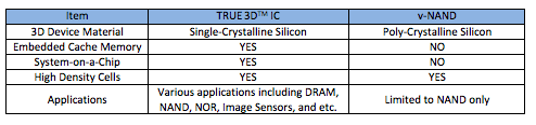
In addition to 3D DRAM, flash memory is also a target application for BeSang’s TRUE 3D IC. As Samsung’s 3D vNAND is also a monolithic 3D structure, I asked Lee to explain how they are different. He explained that 3D vNAND adds multiple poly-crystalline silicon layers to implement NAND cells, whereas TRUE 3D IC adds multiple single-crystalline silicon layers to implements various devices. This table illustrates the differences.
When Samsung announced 3D vNAND flash, I was asked how this would affect the adoption of HMC, and HBM, 3D DRAM technologies. At that time, since 3D vNAND is a non-volatile memory structure an 3D DRAM is a volatile memory structure, each serving different applications, my response was there would be no effect. However, what if, as Hynix claims, 3D DRAM using BeSang’s 3D IC process goes into production next year? This could be a game changer for the 3D DRAM market space.
It’s Lee’s opinion that market overlap between BeSang’s TRUE 3D IC and 3D package with TSV should be small because they are in different domains, and as previously mentioned, they could be used together, thereby maximizing the advantages of both technologies. He says that if very affordable and large amounts of embedded cache memory could be available for CPU or GPU using BeSang’s TRUE 3D IC, it may reduce the demands on 3D packaging because of its advantages such as small form factor, low power dissipation (no I/Os and no parasitics from TSV), high speed (due to millions of via interconnects and no delay from I/Os) and low cost. What that means specifically for HMC, HBM, and DiRAM remains to be seen. ~ F.v.T.


From the BeSang website describing their technology, it looks like the main point is that a thin layer of crystalline silicon is bonded to an underlying wafer that already contains circuitry.
An extremely important aspect is that this crystalline layer does not seem to contain devices at the time of bonding.
The “MaskTo-Wafer” alignment procedure that is highlighted in the website suggests that new active devices will be made in this bonded crystalline layer. Any such devices usually involve the creation of N and P regions that have to be implanted and activated (unless the only devices being added in 3D are metal capacitors/inductors or are restricted to BeSang’s vertical NPN structure embedded in the donor crystalline layer). Creation of active devices involves high temperature thermal steps. This means that the circuitry in the acceptor wafer cannot contain copper or aluminum (only refractory metals such as tungsten can withstand such temperatures). The problem is that the BeSang website contains a basic process flow where the acceptor wafer circuitry does contain aluminum and copper.
There’s the conundrum.
If the acceptor wafer contains copper and/or aluminum, then the process temperatures in making whatever is made in the bonded crystalline layer must be restricted to less than ~400C. This is too low to make standard crystalline devices.
If the crystalline layer already contains fabricated devices (not seen in their website), then the layer must be critically aligned to the acceptor wafer.
Given the above, I am confused as to what BeSang is actually doing.
~ AJW
Francoise
Exellent summary as always. In addition to the great comparison already provided, it might be beneficial to also consider ZiBond(r) Technology as well. This would be a 3D Bonding process probably more aligned to the Besang TRUE 3D IC.
Regarding process temperature, the donor wafer absorbs high temperature annealing process for doping activation before wafer bonding. Also, the donor wafer does not contains pattern to align (There might be some exceptions. However, alignment won’t be an issue at all even in this case). In addition, BeSang’s TRUE 3D IC needs only one mask step to implement transistors in 3D IC layer. (Compare this with 14-17 mask steps for conventional transistor implementation). I want you understand that it is difficult to be more specific.
Sang Yun,
Thank you for responding! I hope this clears up some of the questions.
Rick – Regarding ZiBond – I wasn’t sure if the interconnect was formed by the bond, which is why I was comparing it to DBI, but I was also thinking that ZiBond would be a good process for this application. Sang-Yun was not able to comment on the comparison, because he explained to me that he’s not familiar with the ZiBond process.
Thank you Sang-Yun. Sounds like an interesting concept. It looks like BeSang would be limited to vertical diodes, npn’s and SCR’s since the doped regions have to be uniform across the donor crystalline layer and vertical in orientation. Otherwise, you would need critical alignment. Therefore, with this, I don’t see how more standard elements (FETs, SONOS, floating gate NVM etc) could be integrated in such a 3D stack.
AJW
Francoise
Mr. Lee may benefit by familiarizing himself with our technology. I believe BeSang was introduced to it several years ago and it covers low temperature bonding including a dielectric. ZiBond(R) is simply a homogeneous direct bonding and DBI(R) is a heterogeneous direct bonding where during the process interconnects are formed at the bonded interface. DBI(R) allows for the stacking and interconnecting of active devices without the use of non-CMOS compatible temperatures.
Mr. Lee’s last comment did not address how more standard elements might be included in the process as mentioned by Andrew.
CS