

 I thought I would go to Singapore, attend EPTC (Electronic Packaging Technology Conference 2013) and then take off on my personal vacation to India to attend my 40th high school reunion and 35th college reunion – two weeks tops. It escalated quickly. It ended up being 34 day, 20 city, 6 country marathon. Why you ask? Either I was not willing to give up on the opportunity to meet with packaging thought leaders in Asia, or multiple lapses in judgment. You decide.
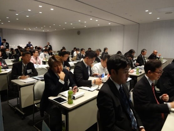
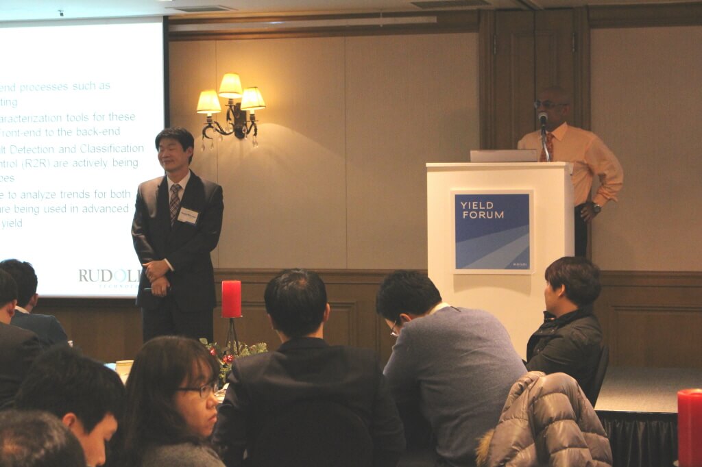
On a positive note, over and above the EPTC, I ended up presenting at the Rudolph Yield Forums in Tokyo and Seoul around that time. Rudolph schedules these highly technical day-long sessions where we present solutions, often with our customers, to leading-edge problems that we are solving in front-end and back-end processes. In Japan and Korea we had around 59 and 100 people attend, respectively.
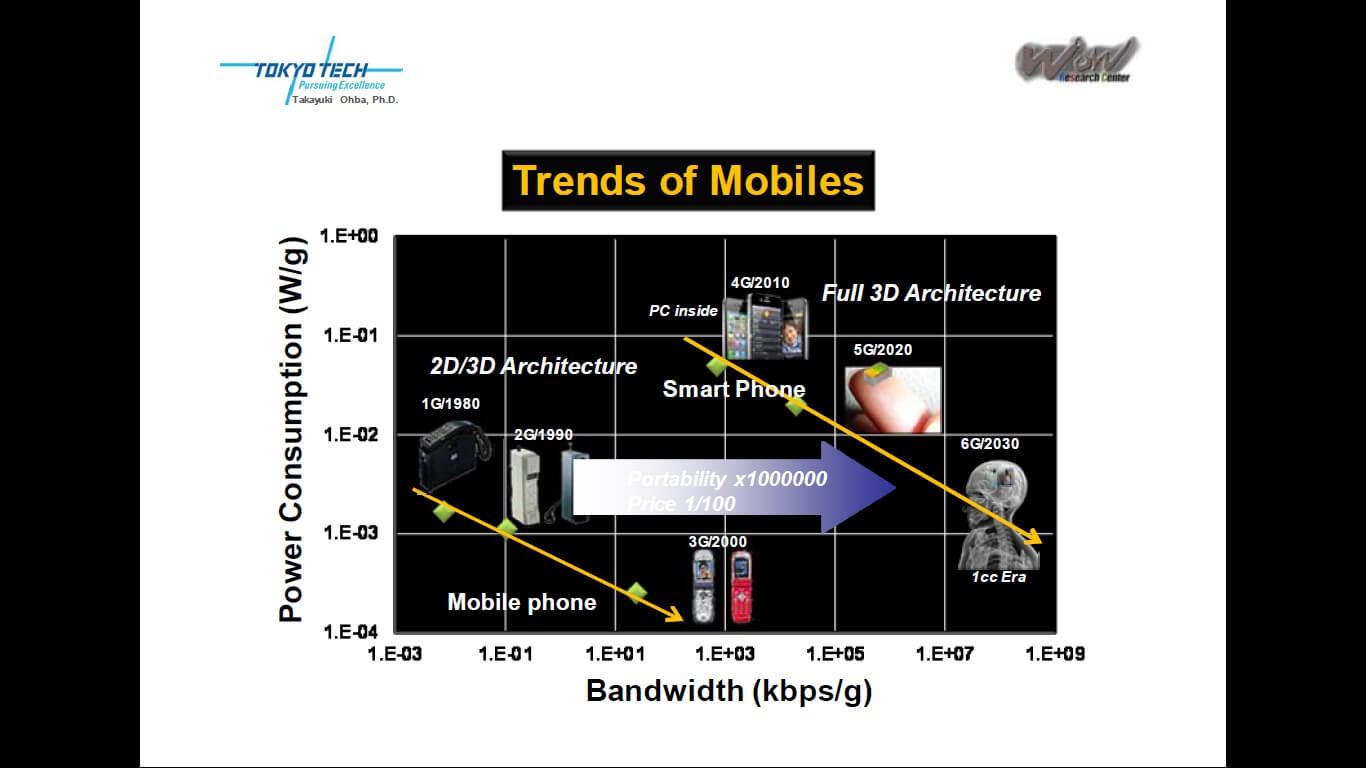 The keynote speaker in Japan was Dr. Takayuki Ohba, a Professor at Tokyo Institute of Technology and associated with the ICE Cube Center WoW 3DI Laboratory, which is a consortium with more than 20 alliance members including University of Tokyo and ITRI Taiwan. He made the case for bump-less connections based on electrical performance and heat-loss based on the lengths of the interconnects. The consortia, as the name suggests is focused on Wafer-on-Wafer based stacking technologies two generations from now.
 From the Rudolph presentations ,a lot of interest was generated on TSV-related Inspection and metrology solutions and lithography for advanced packaging. I had been observing that other typically front-end techniques are inexorably making their way into the back-end – such as multi-layer film thickness and Automated Process Control (APC) techniques like Fault Detection and Classification (FDC) and Run-to-run. In audience surveys this observation seemed to resonate.
Along the lines of everyone that wants to create a new word such as interconnectology, I had called this phenomenon “front-end-ization”. (And fair warning, do not try using it in Words with Friends.) In an off-line discussion with a Singapore packaging manager of an IDM, FDC was already being introduced in key assembly processes such as die-attach and wire-bond. In 2009, I remember making a tour of many advanced packaging houses right after the Rudolph acquisition of Adventa, and APC was being done on Excel spread-sheets if at all! The back-end has rapidly changed in the last few years.
In Korea, Mr. I.B. Park from Amkor provided an insightful case into the packaging trends where the infrastructure for stacked packaging is more robust and ready compared to full-blown 3D TSV. The industry is able to leverage package on package (POP) and fan-out wafer level packaging (FOWLP) to achieve integration of Memory on Logic today.
EPTC was full of interesting announcements and presentations. Great inisght provided by John Lau on the status of TSV. The much cited, Xilinx 28nm based 4 die on interposer had a very specific objective, improve large die yield through partitioning into 4 smaller dies. The next generation part based on 20nm technology from Xilinx, does not need interposers. In other words, John suggests that lateral technology developments may delay interposer adoption out into the future.
 Multiple companies discussed plans for FOWLP – SPIL, ASE and TSMC.
All the companies stated the possibility of FOWLP as a platform for interposers. Interestingly, the TSMC presentation, made by Dr. Toru Ogawa, ex-Sony Japan, now Director of Back-end Business Division showed a very aggressive roadmap for RDL line space and width (5µm/5µm headed to 2µm/2µm). Production ramp is slated for middle 2014. As a reference point, a bulk of high volume FO today is at >10µm line width and spacing.
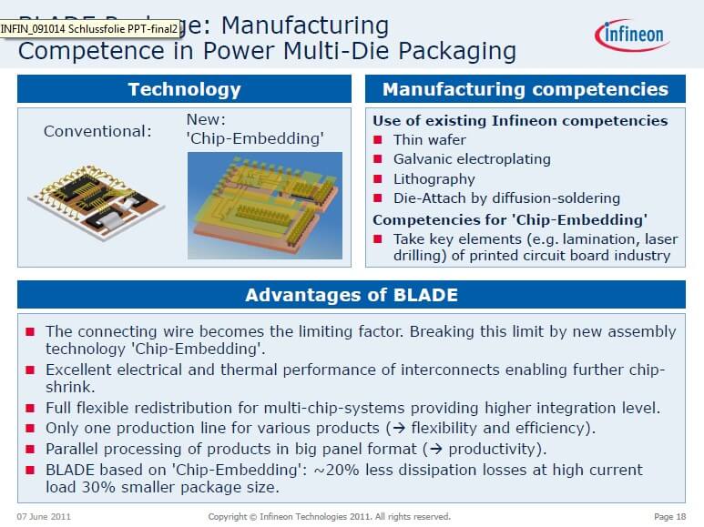 Dr. Hans-Joerg Timme presented the Blade; an embedded die in PCB package. Designed for power applications for the automotive industry, the package offers a 30% foot-print reduction and significant improvement in electrical performance. Yup, fan-out can be implemented in many different ways, embedded die is one of them. Interestingly enough, the Infineon presentation also referred to the leverage of technologies such as lithography and the merging of front-end and back-end technologies for Systems in Package (SiP).
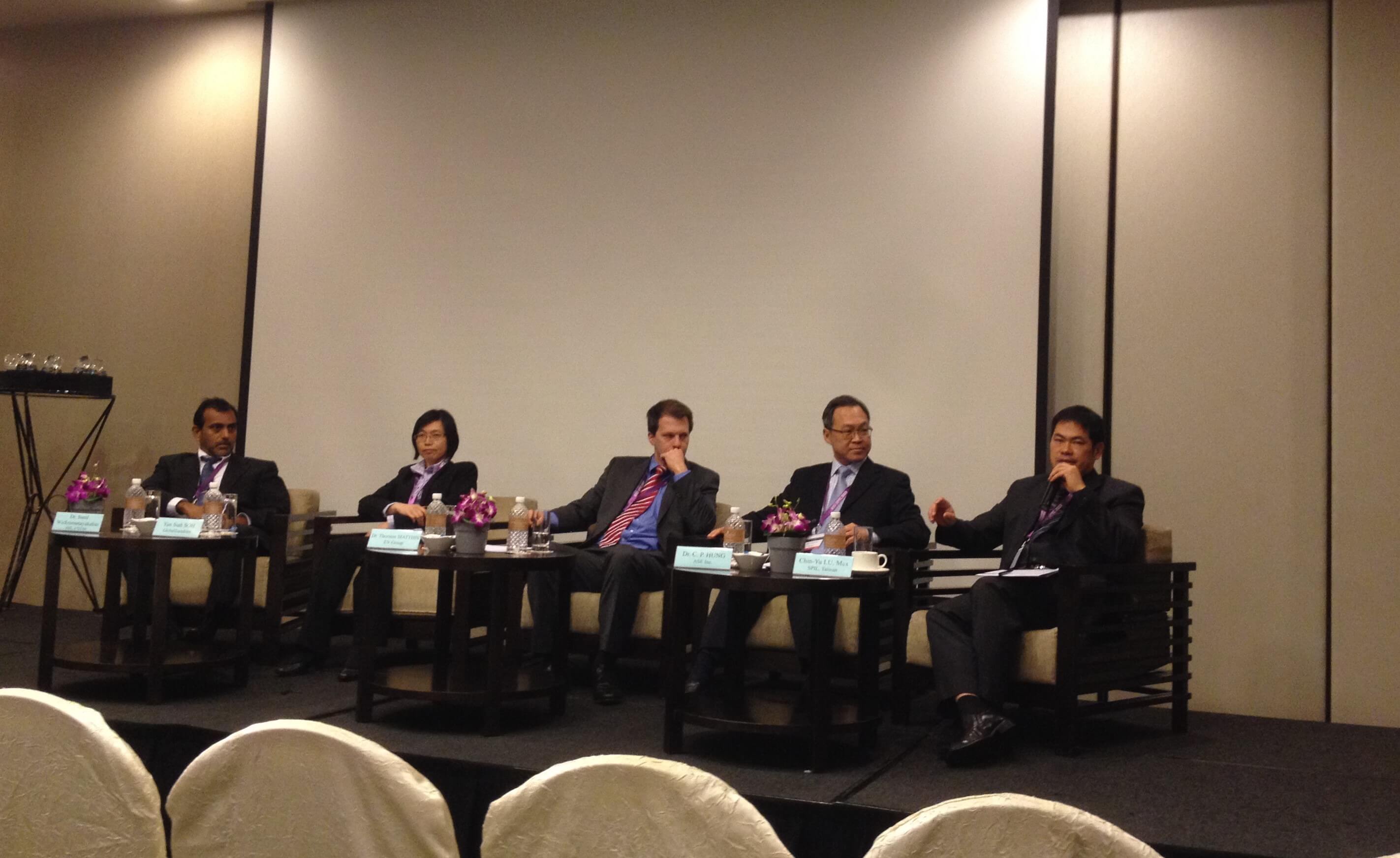
EPTC, incredibly well organized by the local team of packaging experts in Singapore, was intensely technical with an emphasis on package characterization for electrical, mechanical and materials and worth a trip for visitors from Europe and US.
Based on the comments from Infineon, TSMC, ASE and SPIL, I believe we have an exciting 2014 with a number of developments in wafer level packaging and radical new approaches to stacking. ~ R.R


