One of the hottest trends in semiconductor manufacturing today is wafer-level packaging (WLP). According to Allied Market Research, the global WLP market size is expected to reach $7.8 billion by 2022, registering a compound annual growth rate (CAGR) of 21.5% from 2016 to 2022. Broadly defined, WLP encompasses different integration approaches such as fan-in and fan-out, as well as a range of packaging types from 2D and 2.5D to 3D ICs and even nano WLP. It also includes interconnect processes like bumping, through-silicon vias (TSVs), and hybrid bonding.
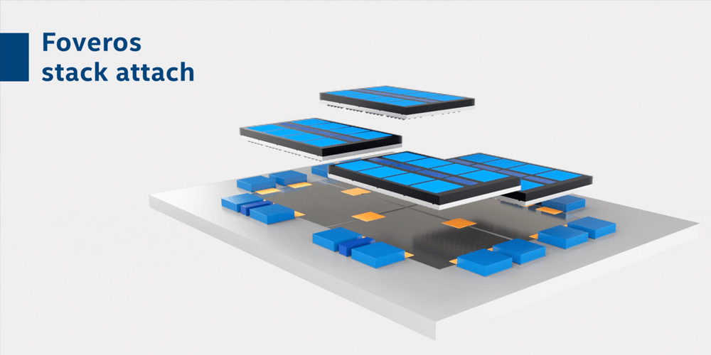
WLP is the cornerstone of heterogeneous integration (HI), which is another of the key trends in semiconductor manufacturing. Many believe that HI is the path to extending Moore’s Law in terms of power, performance, area, and cost (PPAC). HI includes wafer-level system-in-package (SiP) architectures, 2.5 interposers, 3D integrated circuit (IC) stacks, and, most recently, chiplet architectures.
What Is Driving WLP Trends in Semiconductor Manufacturing?
As the pandemic has shown us, the world is depending on digital technologies more than ever. Not only that, but we want the ability to conduct our lives from the palm of our hand. We use our mobile devices to communicate, conduct business, shop, monitor our health and our homes, and more. Heterogeneously integrated WLPs make it possible to pack 5G, artificial intelligence (AI), memory, power, sensors, and more into these tools.
This is driving a demand for WLPs that will continue to increase. At the same time, another industry trend is the focus on sustainable manufacturing to align with the UN’s Sustainable Development Goals. Therefore, not only do we need solutions to support high-volume manufacturing (HVM), those solutions also must be ecologically friendly.
Bring Front-End Processes to the Back End
Unlike traditional chip-packaging approaches, in WLP, everything from chip fabrication to assembly, inspection, and test happens at the wafer level. As devices continue to shrink and technology advances, many of the processes being used are adaptations of those developed for front-end wafer processing. Leading foundries and integrated device manufacturers (IDMs) are leveraging not only know-how but also legacy tools to compete with outsourced semiconductor assembly and test (OSAT) providers for WLP business.
Over the past few decades, one of the trends in semiconductor manufacturing was the proliferation of new tool suppliers who carved a niche for themselves by developing WLP process tools targeted specifically to the OSATs. These tools included those used for:
- Electrochemical plating (ECP) for Cu bump and redistribution layers (RDL) and TSV metallization such as barrier, seed, and fill
- Chemical mechanical processing (CMP) used during the wafer bumping step and for RDL in fan-out wafer-level packaging (FOWLP)
- Wet processing tools used for coating, developing, and plating as well as stripping and etching
This worked well for early iterations of wafer-level packages built using legacy node chips that did not quite need the level of precision and cleanliness required for today’s WLP technologies. Additionally, as OSATs couldn’t easily absorb the cost of front-end tools, systems stripped of all the front-end bells and whistles made it possible for OSATs to add capacity for WLP.
However, as technology nodes continue to shrink, the argument for front-end-level tool capability grows. From high-aspect ratio TSVs and finer bump pitches to tighter RDL line/space widths and precision flatness for hybrid bonding, tools designed for early generations of WLP are not meeting today’s needs for higher levels of precision, uniformity, and contamination control. The bottom line: Wafer-level processes have become much less forgiving and call for tools with front-end processing capabilities. But these tools must still be affordable to keep OSATs in the game. Additionally, as WLP products gain market share, all these processes must be adapted for HVM environments.
![[err-ad-fallback-title]](http://www.3dincites.com/wp-content/plugins/a3-lazy-load/assets/images/lazy_placeholder.gif)
Our WLP Solutions Support Sustainable HVM
At ACM Research, we’ve leveraged our knowledge and expertise in front-end process solutions and adapted them to address today’s high-volume WLP challenges. Moreover, we’ve developed closed-loop systems that require lower chemistry volumes and recycle and reuse chemistries in real time to make the processes eco-friendly.
For example, we figured out how to plate metal films in deep vias or troughs with depths more than 200µm at high plating rates with our ECP ap system. It solves the mass transfer challenge while achieving a better pillar top profile and delivering improved height uniformity at a higher throughput. Its unique wafer-level electric field delivers better uniformity within wafer and within die than conventional ECP tools, while achieving higher throughputs.
Our SFP system is ideal for removing excess copper and the top barrier layer without inducing mechanical stress. Performing hybrid bonding processes such as direct bond interconnect (DBI) requires wafers that are particle free with extremely smooth surfaces. SFP could be an ideal solution for CMP processes used to achieve this. Moreover, wet-etch and dry-etch processes can be integrated into the SFP system.
Lastly, our suite of customizable, high-end wet wafer processing systems supports advanced WLP processes such as copper (Cu) pillar and gold (Au) bumping, as well as TSV, fan-out, and chiplet processes. Tool capabilities include cleaning, coating, developing, photoresist (PR) stripping and etching. In particular, our wet stripping system combines bench-soaking and single-spin PR removal processes in one tool, thereby reducing the amount of chemistry needed for the process.
This is just the tip of the iceberg. To learn more about our full suite of WLP solutions that support today’s trends in semiconductor manufacturing, contact me at jim.straus@acmrcsh.com.