In a previous blog, I discussed a power design network’s (PDN) self and transfer impedances. Self impedance highlights anti-resonances causing a significant increase in the PDN’s impedance. The anti-resonances increase a design’s power, noise, and lessen performance. Transfer impedance shows the change in impedance from one location to another on the PDN structure. The higher transfer impedance indicates higher voltage loss between the two nodes, which is a problem. The PDN is supposed to have the same voltage potential across the PDN.
But there is a third response that needs investigation and it is NOISE. The self and transfer impedances are responses within a given PDN ‘net’. PDN Noise responses are between different nets and can be as troublesome as self and transfer impedances. The noise can either be from different power planes (think of 3.3V vs. 1.8V vs. ‘Gnd’) or between signal lines and power planes. Signal-to-signal noise is part of Signal Integrity metrics and was discussed in other blogs. If insufficient noise isolation (dB) is identified from frequency domain simulation, at a minimum the performance will be degraded with functional failure as worst case. Prof. Swaminathan consistently proposes co –simulating signal AND power integrity analysis.¹ Both affect each other: poor PI affects SI and poor SI affects PI. For deeper SI/PI information, please visit E-SystemDesign website and watch Prof. Swaminathan’s SI/PI video series.
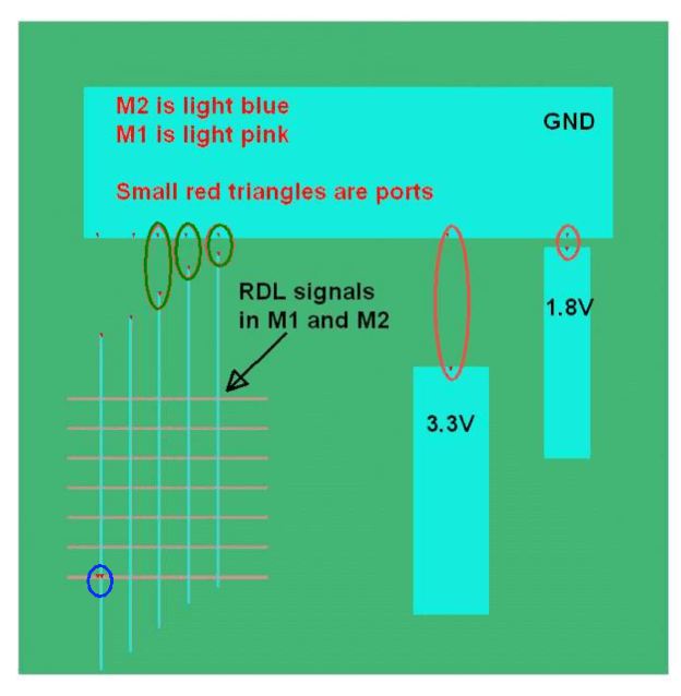
PDN to PDN Noise and PDN to Signal noise structure¹
As discussed in previous 3D InCites blogs, Path Finding allows designers to quickly test various ideas to help separate the viable from the inane. Part of the Path Finding needs to investigate noise between: µvia to µvia, TSV to TSV, signal to signal, PDN to signal, and PDN to PDN. The structure in Figure 1 is a simple test structure (no µvias or TSVs) that I have ported to simulate noise between various ports. The red, green, and blue circles will be the noise responses discussed below. (Er 3.9, LT 0.02, Sigma 5.8e7, metal thickness 0.01 mm and dielectric between M1 and M2 of 0.01mm, all RDL is 0.05mm wide)
What do the simulation results show?
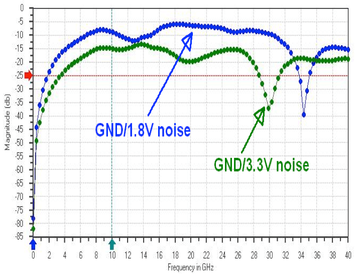
Let us first examine the PDN to PDN noise responses; these are the 2 red circles between GND/1.8V and GND/3.3V shown in the structure above. We could have also examined 1.8V and 3.3V PDN but have not for brevity.
If we set -25dB as the threshold for good noise isolation (-30dB is better), you can see that noise isolation between GND and 1.8V island @ 18 GHz is ~-5dB. The noise isolation is slightly improved between GND and 3.3V island due to increased distance between the planes but is still poor at ~-13dB @ 14 GHz. Both of these have inadequate isolation and additional spacing is required to achieve -25dB.
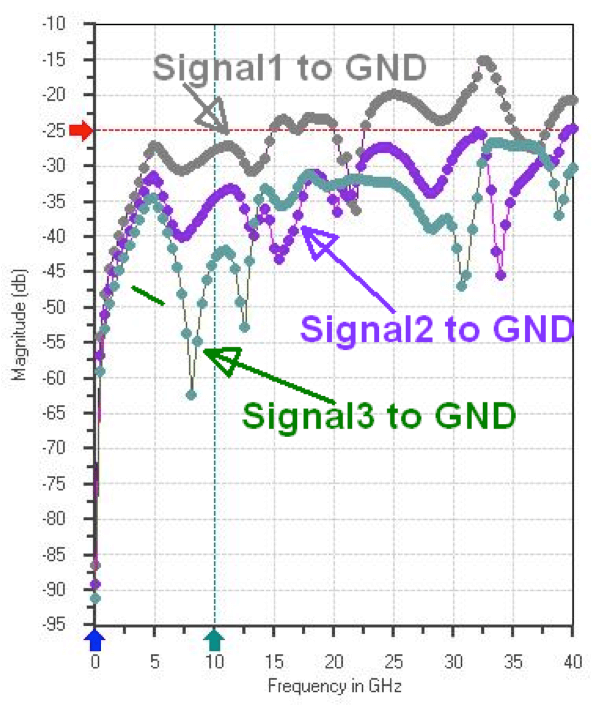
Next, let us look at the PDN to signal noise, these are the 3 green circles between GND and 3 RDL vertical signals shown in the structure above. Signal 1 has the shortest distance to GND plane, Signal 2 is farther away and Signal 3 is the farthest. Again, if -25dB is used as the noise threshold value, we can see that Signal 1 has worse noise and peaks at -15dB @ 33 GHz. Signal 2’s distance from GND plane is sufficient until 39 GHz and Signal 3 also shows improved noise margin until 33+ GHz frequencies. Since the signals are much narrower than the PDN planes in PDN/PDN noise, we have improved noise isolation even though the distance is similar to GND/1.8V planes.

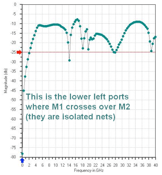
The last check examines signal-to-signal noise where the horizontal RDL crosses over the vertical RDL. We could have examined all of the NEXT and FEXT for the various signal lines, but I wanted to view the noise isolation between two orthogonal signals separated by 0.01 mm. With the same -25dB noise isolation threshold, we can see that these orthogonal lines have significant noise between them (approaching -7dB @ 17 GHz).
Granted this is a small, ‘silly’ example but it shows how noise can affect signal to signal, signal to PDN, and PDN to PDN. Any noise above a defined threshold can cause time to market delays and additional costs. Path Finding allows users to create much larger and more complex structures that can help identify issues long before physical implementation (PCB, package/interposer or IC) is completed. Path Finding construction and simulation is much faster; resulting in significant resources (people, hardware/software) reduction before costly implementation or re-spins are required.
Want additional information?
Technical papers that discuss the Engine behind “3DPF” will be presented at EPEPS (October: San Jose, USA) and EDAPS (December: Seoul, Korea). Two other application related papers will be presented at Zuken Japan (October: Tokyo, Japan) and 3D ASIP (December: San Francisco, USA) conferences. ~ B, Martin
Notes:
1. This is using Sphinx 3D Path Finder (“3DPF”) which is sold and supported by E-SD. In addition, patents are granted and pending.