

CoolCube™: More than a True 3D VLSI Alternative to Scaling
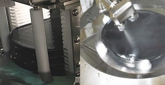
Almost four years ago, we published an article titled “CoolCube™: A True 3DVLSI Alternative to Scaling” on 3D InCites. It described the concept of stacking layers of transistors sequentially on top of each other and documented the research effort happening at Leti to develop a feasible process integration scheme and...
Replacing NMP: Are You Ready?
NMP is an abbreviation for N-methyl-2-pyrrolidone (other synonyms are 1-Methyl-2-pyrrolidone and 1-Methyl-2-pyrrolidinone) (Figure 1). NMP has proven itself as an effective and versatile cleaning agent, removing photoresist residue while leaving the surface in good shape for processing steps downstream. However, its time may be short-lived as companies strive to meet...

The Fundamentals and Early History of Quantum Mechanical Tunneling
The mid-1920’s were the miracle years for quantum mechanics. The “Old Quantum Theory” originating with Niels Bohr, had reached crisis point by the end of 1924. Wave-particle duality from Einstein and de Broglie called for something new. The great theorists, Heisenberg, Born, Jordan, Schrödinger, and Dirac, published different formulations of a new theory that were quickly shown to be equivalent descriptions of quantum...

The Triumph of Quantum Mechanics at the Heart of Solid-State Data Storage
If all the data sent worldwide each day on the internet were burned on to CDs and these were then piled one on top of the other, the resulting heap would reach Mars and back again. Much of this data is thankfully not stored on CDs but rather in much more efficient solid-state memories. And...
Integrated Solid-state Capacitors Based on Carbon Nanostructure
The constant demand for miniaturization, added functionality and increased performance of electronic devices systematically drives higher integration by adding more devices on a single chip. In addition, 3-D or 2.5-D packaging, require on-chip or in-package capacitors, not only in traditional integrated circuits but also for integrated components, possibly on interposers,...
3D Systems-on-Chip: Clever Circuit Partitioning To Extend Moore’s Law
In recent years, the technology of 3D integration has evolved into an economically interesting road. In particular, the technology is used to package the CMOS imagers you find in your smartphone, the high-bandwidth DRAM memory stacks used in high-end computing, as well as in advanced graphics cards. 3D integration allows...

The Dual-Gate Thin Film Transistor for 3D Dynamic and Flash Memory
Data is now the world’s most valuable resource. Solid-state storage of data is driving an innovation revolution built upon 50 years of progress. Here we look at the dual-gate thin film transistor (DG-TFT), an extremely versatile solid-state data storage device that can be used in monolithic 3D as either a flash...
Lam Research: SABRE 3D
SABRE® 3D is a next-generation electroplating product designed to meet leading-edge production requirements for advanced packaging applications. This product leverages proprietary front-end manufacturing technology and offers market-specific solutions for copper pillar and through-silicon via (TSV) fabrication. SABRE 3D offers industry-leading throughput along with reduced cost of consumables to enable high economic value...
Nordson ASYMTEK: Programmable Tilt + Rotate 5-Axis Fluid Dispenser
Nordson ASYMTEK’s programmable Tilt + Rotate 5-Axis Fluid Dispenser dispenses using 5 axes instead of 3. The X and Y tilt enables dispensing from a vertical position, varying tilt angles to all sides of a component and up to the top of a 3D stacked die with high precision and...
SPTS: Sigma fxP PVD with Multi-Wafer Degas
SPTS’s Sigma® fxP, is a well established PVD system used in advanced packaging applications such as UBM and RDL. It utilizes batch degas technology that can improve Rc whilst maintaining high throughputs, despite the outgassing challenges posed from the increasing use of organics, such as mold in Fan-Out WLP. Testimonial...
KLA-Tencor: CIRCL-AP™
CIRCL-AP™ is a cluster tool with multiple modules, covering all-surface inspection, metrology and review at high throughput for efficient advanced wafer level packaging (AWLP) process control. The CIRCL-AP provides production-proven, high sensitivity monitoring capability for multiple AWLP applications including 2.5D/3D integration, wafer-level chip scale packaging and fan-out wafer-level packaging. Testimonial...
EV Group: GEMINI®FB XT Automated Production Fusion Bonding System
The GEMINI®FB XT fusion wafer bonding platform features up to a 3X improvement in wafer-to-wafer bond alignment accuracy as well as a 50% increase in throughput over the previous industry benchmark platform. These performance breakthroughs clear several key hurdles to the industry’s adoption of 3D-IC/TSV technology. Testimonial According to the...

Heterointegration Spoor in the 2015 Analog, MEMS and Sensor Startups to Watch, Part 3
In Parts 1 and 2 of this series, I drew your attention to what Peter Clarke, writing in EETimes on 02 January 2015, called the “15-in-15: Analog, MEMS and sensor startups to watch in 2015.” If we were to look for heterointegration spoor amongst Peter’s 15 notable startups what would...

Executive Viewpoint: Invensas Opens its Toolbox of Interconnect Options
We’ve heard it expressed many times whenever there’s a new interconnect technology vying for adoption: manufacturers will select the best performing option at the lowest cost to do the job. However, as performance requirements reach previously un-anticipated levels, pitch requirements become tighter, and density requirements become higher, the job of...

SSEC: Wet Etch Process for TSV Reveal
SSEC’s wet TSV reveal process achieves -/+ 0.7% Si thickness uniformity under the appropriate post grinding conditions with fast throughput. The two-step process starts with a spin etch for a smooth, fast etch at 10µm/min. The etch is stopped 2µm above the TSVs and then finishes with a selective etch...
Akrion Systems: Vacuum Prime and Dry
Akrion Systems’ vacuum prime and drying technology enables the use of a wet immersion method to introduce liquid chemicals or rinse water throughout the entire HAR feature prior to the oxide etching step. Pulling a vacuum below the saturated vapor pressure of water, draws liquid into the entire feature, enabling...
SETNA: Process for Room Temperature 3D IC Assembly
SETNA, in conjunction with Research Triangle Institute (RTI), has developed a binary alloy (Silver-to-Indium) bonding system for 3D IC assembly that can be compression-bonded at room temperature. Following 3D IC chip stacking, the Ag-In structure is annealed in the solid-state (no melting) to form an Ag₂In interconnect which is stable...
SPTS: Blanket Silicon Etch Process for Via Reveal
The blanket silicon etch process performed on the SPTS Rapier XE achieves an etch rate >8.5µm/min, high selectivity (Si:SiO>150:1), and is ~3-4x faster than competing systems. A unique dual plasma source design creates a uniform etch (<±3%) across a 300mm wafer, which can be “tuned” to compensate for variations in in-coming...
SSEC: WaferEtch TSV Revealer
SSEC’s WaferEtch™ TSV Revealer is a single wafer wet processing platform for 3D IC and interposer wet etching applications designed to reduce processing and capital equipment costs. The WaferEtch features superior uniformity of silicon thickness (as low as -/+ 0.7%). Testimonial Via reveal is a critical process step in 2.5D...
Lasertec: BGM300
The BGM300 was designed to enable quick and accurate measurement of Through Si Via (TSV) depths, Si wafer thickness, and Remaining Si Thickness (RST) above TSVs – all essential in a managed backside via reveal process flow. Back grinding errors due to “blind” grinding can lead to significant yield loss....