


2022 3D InCites Awards Winner Circle
The 2022 3D InCites Awards program recognized industry-wide contributions in the development of heterogeneous integration and 3D technologies. In 2021, we added two awards to recognize companies that demonstrate best practices in sustainable manufacturing efforts, as well as diversity equity and inclusion (DEI). Below are the winners of the 2022 Awards, selected by judges and online vote.
We are delighted to return to an in-person format to celebrate these accomplishments. We presented the awards in a brief ceremony at the IMAPS Device Packaging Conference in Fountain Hills on March 10. If you missed the event, we’ve captured it in photos and a podcast episode.
The Winner’s Circle
Device Manufacturer of the Year:Micross Components
I am very excited to receive this award on behalf of Micross Components. Recognition like this is the culmination of a lot of hard work by our team to develop and deliver the advanced packaging and heterogeneous integration solutions our customers need. Thank you 3D InCites! And thank you to the Micross team, who share this award with me.John Lannon, General Manager, Micross Components
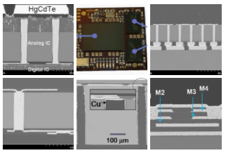
Micross Advanced Interconnect Technology is a leader in 3D integration technology, having developed a broad range of 3D process capabilities and achieved successful demonstrations of 3D-integrated IC stacks for IR focal plane arrays and silicon interposer for embedded computing modules. Micross AIT has been conducting research and development in 3D integration since 1999, building on decades of experience in the development of advanced microfabrication and packaging technologies. Clients can take advantage of the 2.5D/3D integration technology platform to realize more highly integrated microsystems with increased functionality, short interconnect length and decreased size, weight and power (SWaP). From the design and fabrication of custom test vehicles to the application of 3D integration processes modules on fully functional IC wafers, Micross AIT can provide a variety of integration solutions to meet specific project needs.
Device Technology of the Year:AMD
Thanks for choosing AMD for Device Tech of the Year. Our design technology teams are always striving to innovate for the next generation products and our third generation AMD Epyc processor with 3D V-Cache is the industry’s first X86 with true 3D stacking.Raja Swaminathan, Senior Fellow, AMD
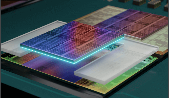
AMD recently released its 3rd generation EPYC processor that implements AMD 3D V-Cache. This is the first true 3D chiplet stacking architecture using the industry’s first copper-to-copper hybrid bonds plus a through-silicon vias (TSVs) approach that provides up to 200 times the interconnect density versus 2D chiplets and approximately 15 times the density versus traditional 3D stacking solutions using solder bumps. The unique bump-less design also consumes less energy than existing 3D approaches. With components placed in a 3D stack for minimum latency, 512increased bandwidth thanks to the tripled L3 cache, and the resultant thermal efficiencies, 3rd Gen AMD EPYC™ processors with AMD 3D V-Cache deliver breakthrough performance, especially for product and engineering design, one of the most compute-intensive workloads.

Engineer of the Year: Dr. Sangki Hong
I’m so happy that 3D InCites selected me as the 2022 3D InCites Engineer of the Year! I am honored to accept this award. I would like to share the award with my colleges at NHanced, who continually support me with their excellent knowledge and experience of 2.5D & 3D integration technology. I would also like to express my appreciation to our valuable partners and customers, who demonstrate faith and trust in us by giving us their 3D development prototyping projects. Our 3D technology endeavors continue to advance. I believe our engineering team will be a key technology provider to the fast growing 2.5/3D industries.
Dr. Sangki Hong, Title, Nhanced Semiconductors
TDr. Sangki Hong has spent most of his long career developing 3D ICs and other advanced packaging. His adventure in 3D began in 2001 with Tezzaron with hands-on development of copper diffusion wafer bonding at the fab in Singapore. He pioneered the technology, ran the fab, trained other engineers, and created patented techniques for alignment and bonding. When the fab moved to US, so did he, continuing to invent 3D bonding miracles. He guided Tezzaron’s creation of 3D stacks of 8 and then 16 wafers.
When NHanced was spun out from Tezzaron in 2017, Dr. Hong took over responsibilities for the fab in North Carolina. He interfaces with dozens of customers and oversees the integration of their 2.5 and 3D designs. He also applies his unique talents to the hard problems of assembling silicon with GaN, GaAs, InP, GaSb, LiNbO, and other materials.
Dr. Hong has developed more than 100 process flows for 3D integration, enabling Advanced Packaging to move beyond prototyping into full production. Learn More
Equipment Supplier of the Year:ERS electronic GmbH
We are very honored to be named Equipment Supplier of the Year. Thank you to the judges panel, the online voters and to everyone who continues to support us. We are proud members of the 3D inCites community and the semiconductor industry, so it means a lot to receive such recognition from our peers.Debbie-Claire Sanchez, FOWLP, FOPLP Business Unit Manager
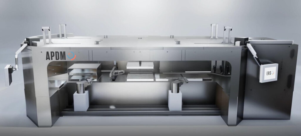
In 2007, ERS developed the first solution for thermal debonding and warpage correction of eWLB packages. 15 years later, ERS continues to support Fan-out technologies with a broader portfolio of automatic, semi-automatic, and manual machines. Combining ERS’s core competencies, these tools address specific challenges in the packaging process, minimizing issues like tape residue, die shift, and handling-induced warpage. They can be found on the production floors of most of the OSATs in the world and are also in use at research institutes, such as Fraunhofer IZM and IME A*Star. In 2021, ERS launched the APDM650 for panels up to 650 x 650 mm, paving the way for high volume manufacturing of large area FOPLP. Their flagship machine, the Automatic Debond Machine (ADM330), is the go-to thermal debond solution in the industry and is continuously being improved to support the ever-evolving complexities of new Fan-out products, with a significant update to be expected later this year.
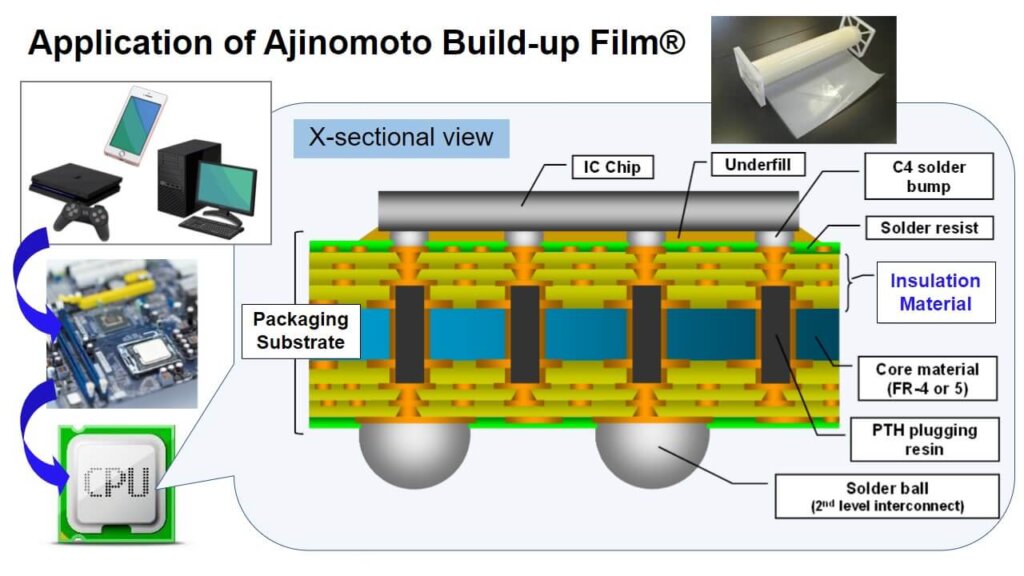
Materials Supplier of the Year: Ajinomoto Fine-Techno Corporation
We are pleased and honored to have been chosen as the winner of the prestigious 3DInCites award for "Material Supplier of the Year"! We are incredibly proud of our Ajinomoto Fine-Techno team for their dedication to inventing cutting-edge materials that benefit our customers. Thank you to the judges and to everyone who cast a vote for us! We'd also want to express our gratitude to the entire 3DInCites team for their hard work!Habib Hichri, Senior Fellow, Global Applications and Business Development, Ajinomoto Fine Techno – USA
Ajinomoto Fine-Techno Co., Inc. (AFT) is a subsidiary of the Ajinomoto Group responsible for the fine chemicals division. AFT (est. 1942) continues to deliver materials that can suit a wide range of customer needs in our four main strengths: molecular design, formulation, process development, and solutions. Our customers have commended us for our electronic materials. We have grown to play a major part in their value chains for electronics, automotive, and a variety of other products. We continue to refine our ability in materials science through research and development to continue creating value with our customers. We strive to provide the highest quality products, services, and information for our customers. Beyond our Ajinomoto Build-up film®, we've expanded our material portfolio to include molding, photo dielectric, magnetic, and optoelectronics.
The Herb Reiter Design Tool Award:Cadence
Thanks for the award. Thank you to 3D InCites, and thank you to all the people who voted for us. We’re pretty excited. It’s good to see our product being recognized like this. John Park, Product Management Group Director for IC packaging and cross-psolutions at Cadence Design Systemsitle or position in a company
Cadence made an unprecedented leap in the industry, advancing 3D-IC design with its Integrity 3D-IC platform. The new platform is the industry’s first comprehensive, high-capacity 3D-IC platform that provides system planning, chip and package 3D implementation and integrated electrothermal, static timing analysis (STA) and physical verification flows in a single cockpit, enabling faster, high-quality 3D design closure.
Legacy market solutions were disjointed, utilizing a die-by-die implementation approach. To differentiate, Cadence enhanced its system-on-chip (SoC) implementation with 3D partitioning and tightly integrated system analysis tools around a multi-technology database to give customers an additional benefit of system-driven power, performance and area (PPA) optimization.
This next-generation platform is for designers creating tomorrow’s multi-chiplet designs for hyperscale computing, 5G communications, mobile and automotive applications.
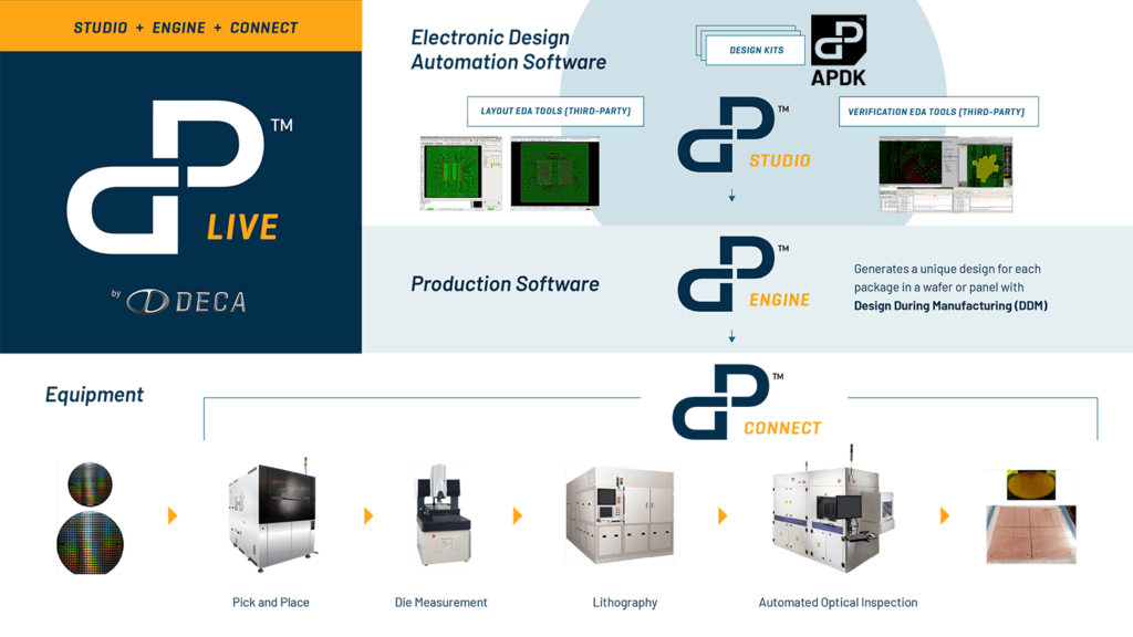
Process of the Year:Adaptive Patterning – Deca Technologies
We are incredibly honored to have Adaptive Patterning selected as this year’s 3DInCites Process of the Year. Thank you to the judges and all of those that voted for us this year! We are proud of our Deca team for all that we’ve
accomplished and we look forward to the exciting possibilities Adaptive Patterning brings to future generations of chips everywhere.
Craig Bishop, , CTO, Deca Technologies
Deca’s Adaptive Patterning (AP) technology liberates designers and manufacturers from the constraints of fixed photomasks, allowing the production flow to account for natural variation without costly processes or design limitations. By combining a high-speed and accurate optical position inspection with a scalable computing cluster, AP generates a bespoke layout for each individual device that compensates for measured positional error. After each pattern is generated, it is converted into digital exposure data for implementation with maskless laser direct imaging (LDI) equipment.
In the previous year, Adaptive Patterning has been implemented, proven, and ramped into high volume production for 600mm FO-PLP. This major accomplishment attests to the power of AP to overcome the challenging die-shift problem of large formats. With the removal of natural variation by Adaptive Patterning, fine-pitch heterogeneous integration at the scale of panel-level manufacturing is becoming reality. Learn More
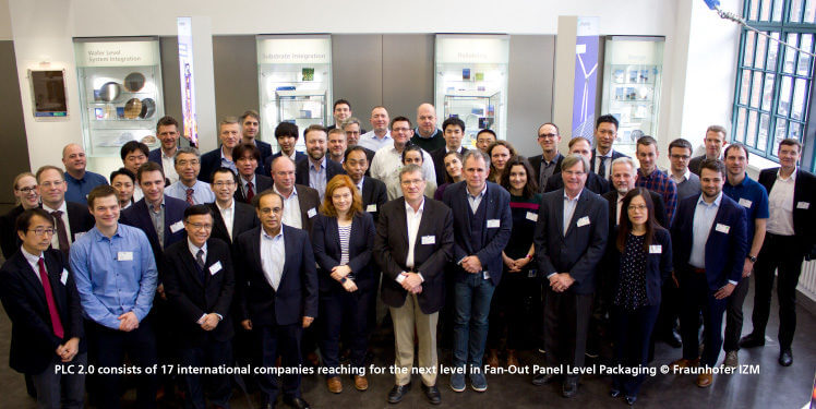
Research Institute of the Year: Fraunhofer IZM: Panel Level Packaging Consortium 2.0
We’re honored to receive this award as a consortium for the second time! We take it as a recognition of the multidisciplinary work we have been able to do within the consortium to advance the PLP technologies towards a high performance platform for microelectronics integration.Dr. Tanja Braun, Group Leader, Fraunhofer Institute for Reliability and Microintegration IZM
In 2016, Fraunhofer IZM teamed up with a group of industry leaders from Europe, the US, and Asia to develop the fundamental processes for new PLP technologies that are ready to transition to industrial-scale high-volume production.
With the second consortium launched for 2020–2022, again with 17 industry partners, the focus has shifted to investigating the physical limits of fan-out panel level packaging (FOPLP). This includes topics like warpage and die shift, adaptive patterning, ultra-fine-line wiring down to 2 µm L/S with a potential move to 1 µm. Migration effects of fine line wiring are also investigated. Cost and environmental modelling accompany the technological research.
New equipment for PLP has been installed and the project benefits from several major investments made by the German Government, allowing Fraunhofer IZM to establish a unique PLP infrastructure for current and future research topics. Learn More
Startup of the Year:Mosaic Microsystems
“We are honored to be selected as “Start-up of the Year” by the 3D InCites Awards panel and the community votes. As a start-up in Advanced Packaging, we are grateful for the recognition and proud to be a part of this dynamic community. Thank you to the 3D InCites team for creating this platform for recognition, and to everyone who voted for us!”Shelby Nelson, CTO, Mosaic Microsystems
Founded in 2016, Mosaic Microsystems is a reliable source for thin glass interposers for microelectronic, photonic, RF/mmWave, MEMs and sensor technologies. Mosaic first leased cleanroom space in 2019, and has been shipping glass wafer products ever since. By 2022, Mosaic has grown to a technical team of nine, with experienced leadership from successful serial entrepreneur and CEO, Christine Whitman.
Mosaic’s thin glass wafers with precision through-glass vias (TGVs), are available in a range of integration levels. The simplest are thin TGV glass wafers, made either of fused silica or of glass thermally matched to silicon, bonded to a handle wafer with Mosaic’s proprietary Viaffirm® bond. Viaffirm is stable to temperatures over 400⁰ C, opening up the parameter space that can be used for top surface metallization and passive devices. Mosaic also provides void-free copper via-fill and RDLs, and works closely with customers to provide unique solutions for advanced packaging.
SemiSister Award for DEI:AMD
It’s really an honor, on behalf of the global AMD team, to accept this SemiSister Award for DEI. AMD has been committed to growing diversity, equity and inclusion in our workforce to drive innovation and foster creativity. The diverse mix of employees with different viewpoints and experiences will a key driver that contributes to our ability to build the next great product. We are extremely proud our diverse teams all over the globe. Raja Swaminathan, Senior Fellow, AMD
AMD continues to strive for high performance in both its products and people. The company believes embracing differences amongst employees is the best way to foster a more creative and collaborative workforce – and drive business performance. They have been recognized by their equality efforts in both the Bloomberg Gender-Equality Index (GEI) and Human Rights Campaign’s (HRC) Corporate Equality Index. These two achievements highlight AMD’s commitment to building a more equitable workplace for its employees.
“We are incredibly proud that AMD was again listed in the Bloomberg Gender-Equality Index and Human Rights Campaign Corporate Equality Index. AMD is committed to attracting, hiring, developing, and retaining the best talent in the industry." Learn More

Sustainability Award:EMD Electronics
We are delighted to receive the 2022 Sustainability Award from 3D Incites, which is a great recognition of EMD Electronics’ commitment to and relentless efforts in sustainability. We strive to embed sustainable thinking in our processes and products, and are committed to foster best practices in promoting sustainable semiconductor manufacturing. Under the framework of our well-established goals and initiatives, we will continue to work with our customers and partners to optimize a sustainable value chain in the semiconductor industry.Anand Nambiar, Executive Vice President, Semiconductor Materials, EMD Electronics
We want to create long-term added value for society, which is why we have defined three goals within our sustainability strategy: In 2030, we will achieve human progress for more than one billion people through sustainable science and technology. By 2030, we will integrate sustainability into all our value chains.
By 2040, we will achieve climate neutrality and reduce our resource consumption.
Out of 17 SDGs in total, we contribute the most to the following five SDGs with our business and our behavior:
SDG 3: Health and well-being
SDG 8: Decent work and economic growth
SDG 9: Industry, innovation and infrastructure
SDG 12: Responsible consumption and production
SDG 17: Partnerships for the goals
In addition, our management approaches and projects also support SDG 4 (Quality Education), SDG 5 (Gender equality) – supplemented by diversity and inclusion, SDG 6 (Clean water and sanitation), SDG 7 (Affordable and clean energy), and SDG 13 (Climate action).
Learn More