
Samsung Foundry Forum
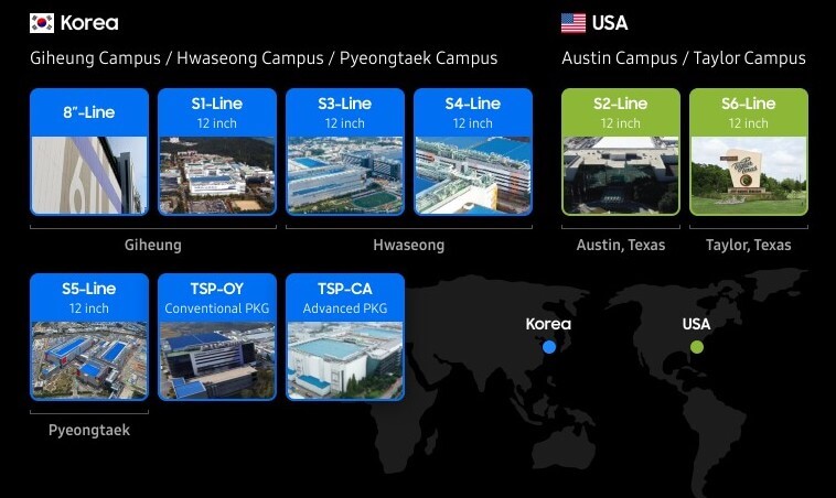
Moonsoo Kang, Head of Business Development at Samsung Foundry, at the 2022 Samsung Foundry Forum (SFF) explained that they would be using advanced heterogeneous integration as a method of streamlining and improving the process of integrating separately manufactured chip components into a single assembly level. Figure 1 shows a listing of Samsung Foundry manufacturing sites in Korea and the US.
Kang presented detail on the company’s roadmap for its advanced heterogeneous integration solutions. Kang noted that as the industry has reached the maximum reticle size that can be printed at once using photolithography, scaling cannot be relied on as the sole solution for high-performing chips.
Samsung also will be relying on chiplet technology in the future noting that by partitioning a large die into smaller chiplets and adopting an optimal process for each chiplet, they hope to improve overall yield and reduce manufacturing costs.
Their customers have also explored the benefits of reusing chiplets. Reusing most of the IP in a product as chiplets, redesigning only the excluded area, and then combining it all using heterogeneous integration techniques can result in significant time and cost reductions.
Kang also gave details on the advanced package technologies that are powering new Samsung advanced packaging integration. These advanced package technologies (which they call “Cubes”) – based on both horizontal and vertical integration have been labeled I-Cube, H-Cube and X-Cube.
- I-Cube is a 2.5D solution, which places chips horizontally on top of an interposer. Samsung offers two types of I-Cube: I-CubeS and I-CubeE. “I-CubeS 8 has an interposer made of silicon and features a 3x reticle size to carry eight HBMs and two logic dies,”. I-CubeE, (Embedded Silicon Bridge) is a more cost-effective option for large interposers. He noted that they plan to expand the size of I-CubeE so that it can integrate up to 12 HBMs for mass production in 2025.”
- H-Cube (Hybrid Cube) is another 2.5D solution. This solution converts large ABF substrates into a combination of a smaller ABF substrate or FBGA substrate and a larger HDI substrate.
- X-Cube is a full 3D solution, which allows the vertical stacking of chips. X-Cube comes in two different forms: Two vertically stacked dies are connected either with micro-bumps, or by bump-less Cu-to-Cu direct bonding. They plan to start mass production of X-Cube products with micro-bump type in 2024, and bump-less type in 2026.
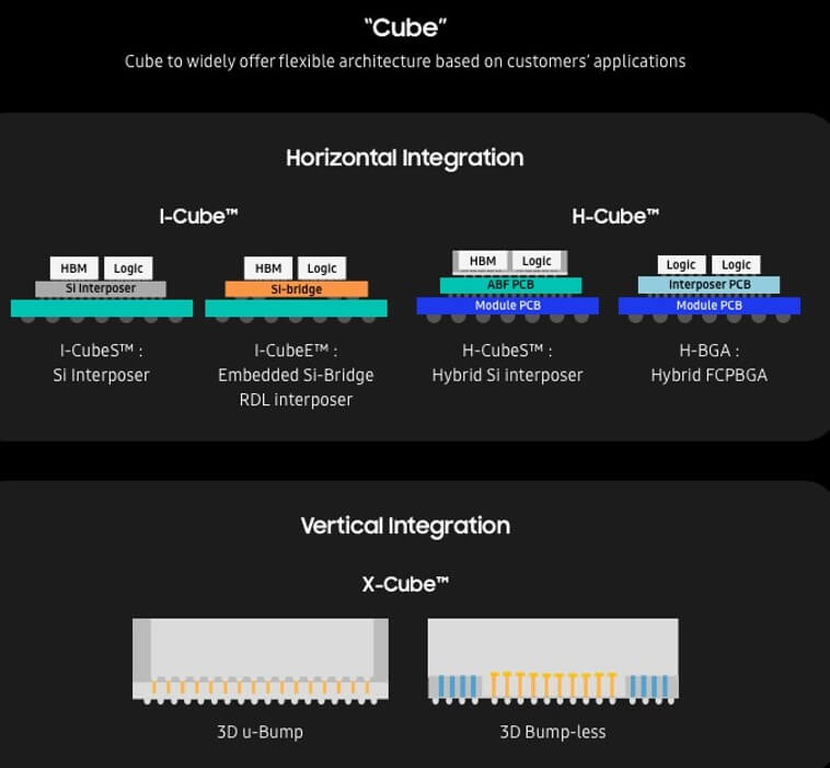
Figure 2: Samsung Foundry’s advanced heterogeneous integration.
Other Advancements and the Growth of a Seamless Ecosystem
Beyond Cube solutions, Kang detailed the other technologies and advancements that Samsung Foundry has been focusing on including direct 3D stacked DRAM on a logic die (in collaboration with the Samsung Memory Division) without a buffer die, to support the next generation of high-performance computing (HPC) devices.
Kang noted that “Our ecosystem for ‘Beyond Moore’ today includes a large number of partners, such as Design Solution Partners (DSP), IP vendors, EDA partners, OSATs, and even PCB suppliers. By closely collaborating with our eco partners, we will accommodate a host of different business models and customer needs and provide seamless support in a highly flexible way.”
Samsung Foundry Business Growing
Samsung Foundry, the global No. 2 foundry, is reportedly closing in on TSMC in the foundry business.
The company currently operates or plans to add foundry facilities in Hwaseong, Giheung, and Pyeongtaek in Korea and Austin and Taylor in the United States.

For the first time in the industry, Samsung began producing chips using 3nm technology in June 2022 by applying gate-all-around (GAA) transistor architecture. The company aims to apply 2nm technology in 2025 and 1.4nm technology in 2027.
Qualcomm, Tesla, AMD as well as many firms in high-performance computing, network, and automotive industries are sending orders to Samsung to produce their chips. Thanks to its efforts to secure more clients, Samsung’s foundry customers more than doubled in 2022 compared to 2019 and the number is expected to increase more than five times in 2027.
Amkor / GlobalFoundries to Provide Semiconductor Test and Assembly Services in Europe
Amkor and GlobalFoundries have recently announced that the two companies have formed a strategic partnership to enable a comprehensive EU/US supply chain from semiconductor wafer production at GF to OSAT* services at Amkor’s site in Porto, Portugal.
Amkor is currently the only high-volume, “Tier 1” OSAT in Europe, and GF Dresden is Europe’s largest and most advanced semiconductor manufacturing services company.
GF plans to transfer its 300mm Bump and Sort lines from its Dresden site to Amkor’s Porto operations to establish the first at-scale back-end facility in Europe. GF will maintain ownership of its transferred tools, processes, and IP in Porto. Both partners also plan to collaborate on future development efforts in Portugal.
For all the latest on Advanced Packaging stay linked to IFTLE……………………………


