
The decline of centralized semiconductor industry R&D labs, as well as the technical challenges facing semiconductor manufacturers, have helped the rise of independent research and development institutions. These organizations such as imec and CEA-LETI, both in Europe, are funded in part by local and regional governments, but more importantly, they are funded by companies either performing pre-competitive research with the R&D centers as the primary project manager, or companies that choose to use imec or Leti as an extension of their research centers and use the R&D centers resources in addition to those of their own.
imec and CEA-Leti both have opportunities for outsiders to learn about what is taking place inside their facilities. CEA-Leti’s event is coming up on June 21-23 at the Leti Innovation Days 2022, in Grenoble France. imec held its annual Future Summits in Antwerp Belgium May 17-18. The imec event had multiple emphases, with the ITF Belgium, Deep Tech Dive, Knowledge for Growth 2022, life sciences conference, and Business Fast Forward.
imec pulled together a stellar program, featuring Pat Gelsinger, Peter Wennink, Tim Archer, Paul Stoffels, Lars Reger, and Ursula von der Leyen the President of the European Commission.
One of the consistencies of the imec forums is that they keep us focused on the issues that are facing the industry. One could say that the International Technology Roadmap on Semiconductors (ITRS), or Sematech used to keep the industry focused, but it seems now that imec has taken over that role.
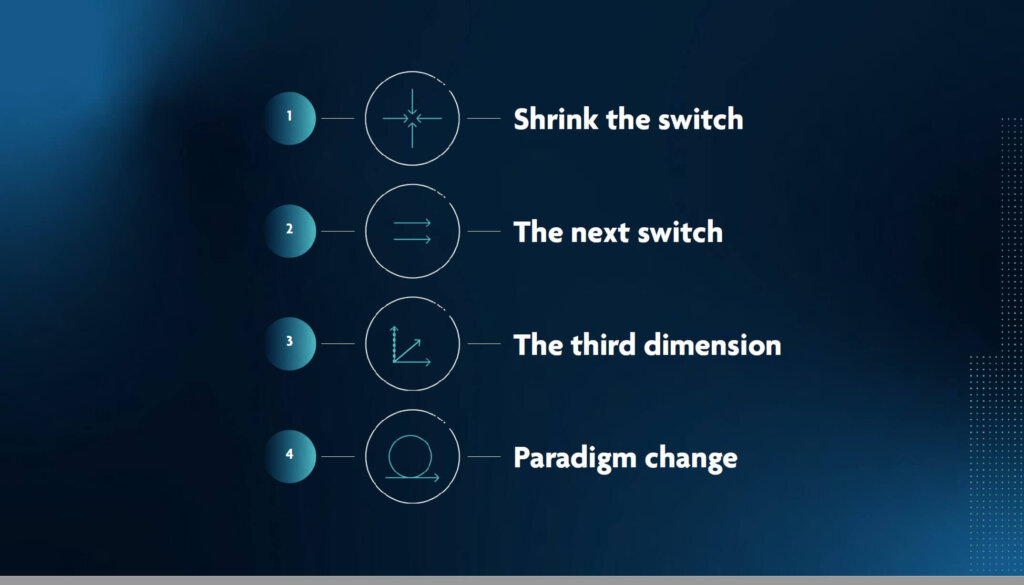
Figure 1: imec’s big picture perspective (source imec ITF Belgium)
But whereas the ITRS kept the industry focused on linewidths, and the red brick wall, (technology challenges needing to be overcome), imec sets up the programs that enable the industry to overcome the next-generation challenges. Figure 1 shows from the big picture perspective that imec considers some of the key issues to be:
- Shrink the switch
- Scaling needs to continue
- Thus EUV, new transistor, and metallization programs
- The next switch
- Moving to new transistor types, monolithic silicon, and 2D materials
- The third dimension
- 3D packaging, and 3D memory and logic
- Paradigm change
- System-level thinking
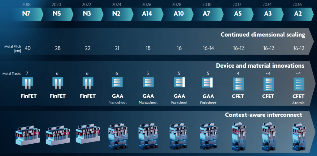
imec is very proactive about sharing its thoughts on what it thinks the next-generation transistor or metallization should look like, and the industry in most cases follows this roadmap, not always to the letter, but pretty close (Figure 2). This can be observed by companies having introduced hi-k metal gates, gate all around transistors, and buried rail metallization technology into production, or their roadmaps for chip technology, after having participated in imec programs.
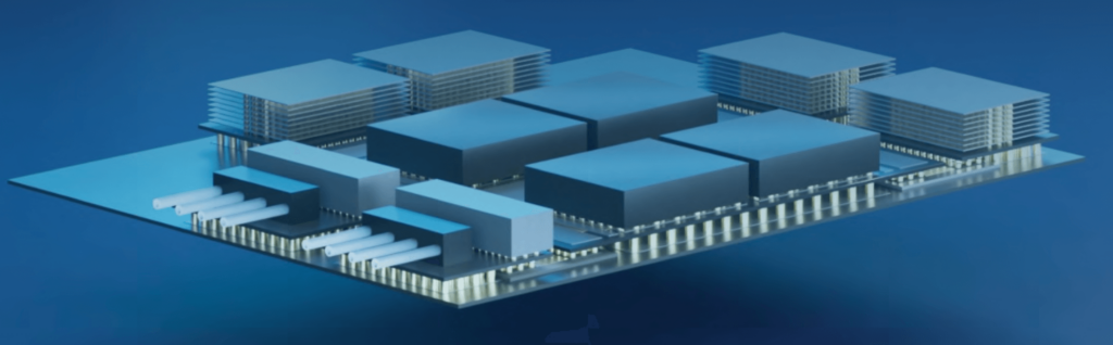
Focusing on semiconductor industry R&D for 3D
But, in today’s electronics with the system on chip reaching the limits of its effectiveness, the need for 3D heterogeneous systems is very real. While according to Eric Beyne, there are certain aspects of 3D the industry is fairly comfortable with such as stacking DRAM, the stacking of logic, analog, and memory in the same package still have some challenges to overcome. One of those is bump pitch, and the other is considering how a system should fit together, and the optimal way to create and design the system in a package (SiP). Some of the AI chips in development are beginning to adopt system-level thinking (Figure 3). This type of design consideration will become considerably more important as edge compute and the need for better energy conservation in chips and systems is adopted.

An area that doesn’t get much press is how imec has been instrumental in the marriage of technology and medicine. In his keynote, Luc Van Den Hove pointed out how technology is enabling medicine, which will hopefully make medicine more affordable and available in the future. The amount of work imec is performing in the medical space is extraordinary and continues to grow with the organization. This includes sensing, fluidics, improving detection techniques, such as moving from manual to automated detection, neuroscience, and more. It is a considerable portion of imec’s research with the goal of digitizing medicine and helping to speed up the time it takes to find solutions to the medical challenges facing the world.
Imec has also launched a new deep tech venture, that they term Xpand. Historically, imec has focused on bringing new technology to its partners and collaborators. The technology developed in imec’s programs would typically be licensed, at no charge to the partners that participated in the research. Since 1986 imec has launched 40 spinoff companies. With the need for new deep tech solutions becoming greater, imec is launching both a venture arm and a startup incubator to help new ideas get off the ground and become commercialized.
XPAND-I has a 177-million-euro fund that is working with 15 portfolio companies that have had six successful next investments. XPAND-II had its first closing with 150 million euros and is targeting 250 million euros in total investment. The proposed model is in figure 4.
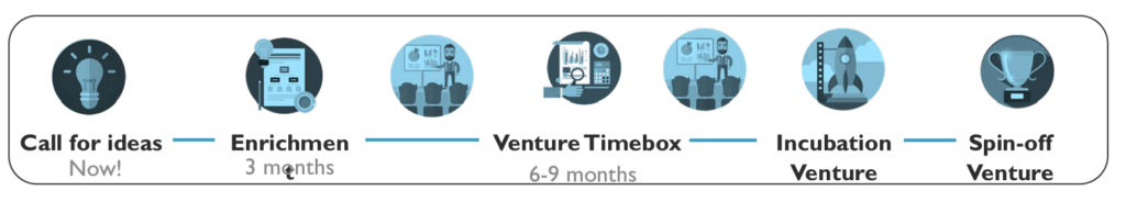
Xpand and its counterpart accelerator, istart, provide a unique opportunity for entrepreneurs with deep tech start-up ideas. While the ideas will need to make it past the culling phase once inside, they have access to a start-of-the-art laboratory, as well as researchers that have been focused on deep tech issues for many years. Thus far, out of 198 start-ups, 25 have had exits and have generated 120 million euros in revenue. imec’s venture also provides a unique opportunity for semiconductor startups that many times have challenges raising VC dollars. Thus, imec not only keeps the semiconductor industry rolling along with the pre-competitive research programs it manages for the industry, but it also ensures that new ideas created by entrepreneurs can be developed into the next big thing that can benefit the IC industry.


