

Finishing up our look at the 2021 IEEE ISSCC, Forum 5 was entitled Enabling New System Architectures with 2.5D, 3D, and Chiplets. This was another clear example of a here-to-fore front-end conference now focusing on advanced packaging technologies. The session description states “The end of scaling drives innovative 2.5D, 3D and chiplet technologies to extend Moore’s law. Advancements in multi-die integration effectively reduce costs at advanced nodes while providing flexibility, modularity and heterogeneous integration…designers need to rethink system architectures to exploit these advantages.”
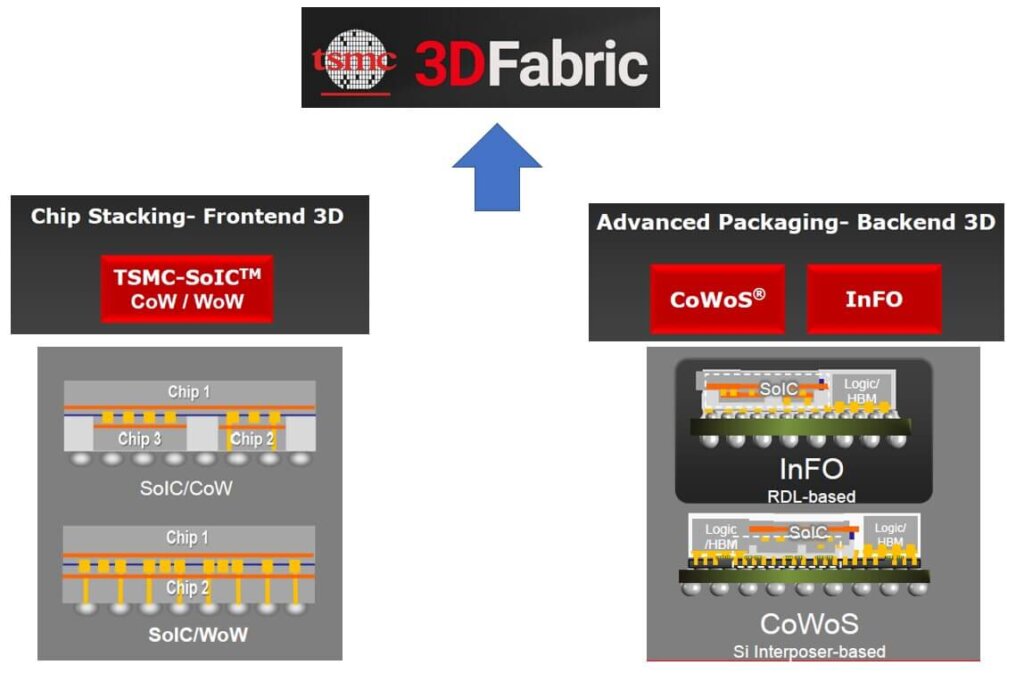
TSMC’s 3D Fabric
Doug Yu of TSMC discussed Foundry Solutions for 2.5 / 3D Integration”. TSMC has rebranded its leading chip packaging technologies as 3D Fabric as shown in Figure 1. If you’re not familiar with the acronyms, catch up on reading past IFTLE reports on TSMC!
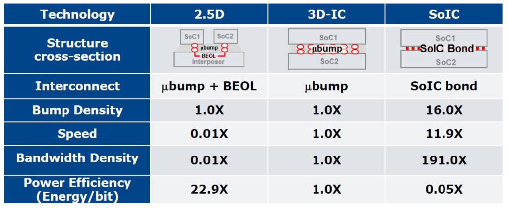
SoIC is compared to 2.5D and 3D in Figure 2.
Yu concluded with a 3D Interconnect density roadmap for the future.
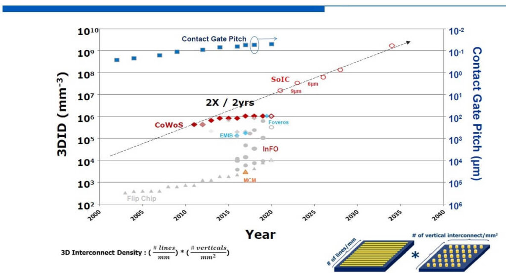
Figure 3: Interconnect density roadmap. (Courtesy of TSMC).
Samsung’s 2021 IEEE ISSCC Presentation
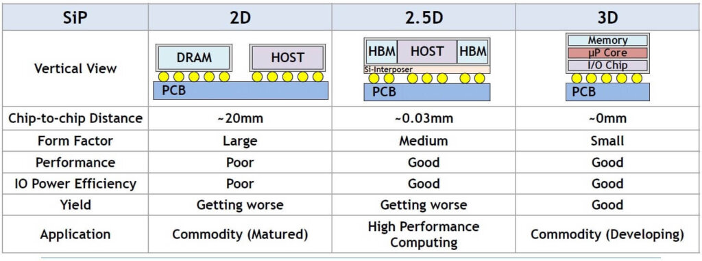
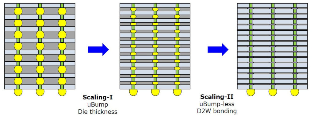
Kyomin Sohn of Samsung discussed 3D stacked memory architecture with 2.5D Heterogeneous Integration. Sohn looks to 3DIC for higher performance, lower power, smaller form factor, and higher yield (3D).
He sees memory stacking moving from micro-bumps to “µ-bumpless D2W bonding” (If you’re a reader of IFTLE you know this is as Ziptronix / Xperi DBI™ Ultra or hybrid bonding)
Samsung lists the following design challenge for 3D stacked high bandwidth memory:

- Performance limitation
- Power dissipations — Thermal throttling
- 3D die-to-die variations — Performance loss
- Harsh 3D operation environment
- Thermal coupling — Memory bit-cell failure
- Huge current consumption — IR-drop induced function failure
- Test and validation limitation
- KGD business model — Incomplete test
- Limited access during debugging — Time-consuming analysis
Sony’s 2021 IEEE ISSCC Presentation
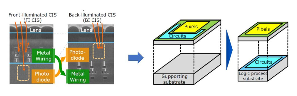
Yusuke Oike of Sony discussed Evolving Image Sensor Architecture through Stacking Devices. Stacked CMOS image sensors (CIS) are now standard in nearly all smartphone cameras. It has been nearly 15 years since the industry began to adopt back side illumination, which was followed by the separation and stacking of pixels and circuits. Connections were accomplished by direct copper – copper hybrid bonding technology making CIS the first application to use this technology. (see Samsung discussion above)
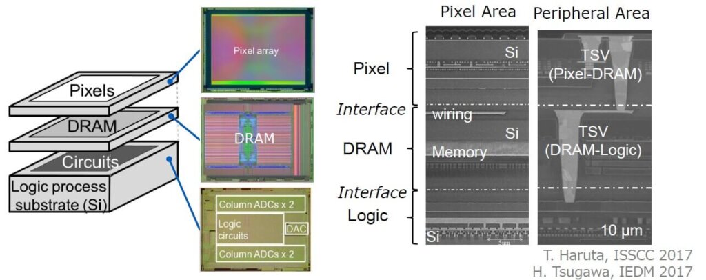
Then a few years ago Sony was the first to include DRAM into the stack for its slow-motion capture applications.
Oike then described how sensor architecture is evolving using 3D technologies:
- More advanced pixel circuitry
- Stacked pixel circuitry
- Event-based vision sensing
- Pixel-parallel ADC architecture
- SPAD-based photon counting
- Hybrid Integration on Si
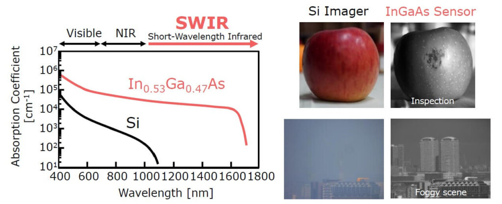
- SWIR InGaAs photodetector
- Integrating more intelligent processor with sensor
- Intelligent vision sensor
For example, the use of InGaAs sensors for future automated inspection and security cameras.
For all the latest in Advanced Packaging stay linked to IFTLE……………………….


