


The 2020 3D InCites Awards program has been a bit of a nail biter for us all, as we waited for the judges’ votes to see how they aligned with the online votes. Remember: the online votes serve as one judge. So, it was possible to win the online vote yet still not win the award. That turned out to be the case in several categories, where the judges were quite divided in their decision. In others, the online vote was the tiebreaker. So, thank you to all who voted. Your contributions helped us make some tough calls.
First of all, a big thank you to our elite panel of judges, Jan Vardaman, Mike Pinelis, Rozalia Beica, and Jean-Christoph Eloy, who volunteered their time to review the nominees and make careful selections. This was was NOT an easy decision to make. In fact, some of the races were so close, I decided to also acknowledge the runners up in this blog. All of the nominees have made significant contributions to the industry and should all be acknowledged for their work in furthering the commercialization of heterogeneous and 3D integration technologies. Without them, emerging technologies like artificial intelligence (AI), machine learning (ML), and 5G would still be at the concept stage. I am continually amazed at how the brilliant minds in this industry come together as a community to solve what often appears to be insurmountable challenges.
Winners of the 2020 3D InCites Awards by Category:
Design Tool Provider of the Year: zGlue ChipBuilder
Runner Up Coventor 3D Semulator
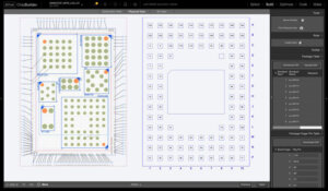 zGlue and Coventor were in a dead heat, and in a last-minute race to the online poll, zGlue edged past Coventor for the win. ChipBuilder 2.0 is an enhanced design tool that allows you to build custom silicon chips in three simple steps. Just select chiplets from an expanded library, capture schematics, route the design with automated verification, and download your netlist. In a single tool, you can view realistic 3D models, download a customized software development kit (SDK) and start coding. Then place an order for manufacturing through the zGlue Shuttle Program. zGlue won the 2020 CES Innovation Award. zGlue is also part of the Chiplet Design Exchange, a subproject to the Open Compute Project tasked with standardizing machine-readable chiplet models to enable chiplet catalogs and provide reference flows for the development of chiplet-based modules.
Device Manufacturer of the Year: Omnivision
Runner Up: StratEdge
![]() This one was a tie, coming down to the actual number of votes. StratEdge came in a very close second. OmniVision’s CMOS imaging technology enables superior image quality in many of today’s consumer and commercial applications, including mobile, automotive, security, IoT/emerging, computing, and medical. The company recently achieved the Guinness World Record for the smallest commercially available image sensor with our medical sensor that reduces invasive procedures and cross-contamination for disposable endoscopic applications. Omnivision also launched the automotive industry’s first high-resolution sensors with HDR, LFM, and cybersecurity, assisting in a safer driving experience with the latest imaging technologies.
This one was a tie, coming down to the actual number of votes. StratEdge came in a very close second. OmniVision’s CMOS imaging technology enables superior image quality in many of today’s consumer and commercial applications, including mobile, automotive, security, IoT/emerging, computing, and medical. The company recently achieved the Guinness World Record for the smallest commercially available image sensor with our medical sensor that reduces invasive procedures and cross-contamination for disposable endoscopic applications. Omnivision also launched the automotive industry’s first high-resolution sensors with HDR, LFM, and cybersecurity, assisting in a safer driving experience with the latest imaging technologies.
Device Technology of the Year: TSMC’s SoIC™
Runner Up: SmartSens
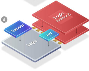 Here the people and the judges agreed: TSMC’s bump-less System on Integrated Chip (SoIC™) is a game-changer. Like InFO did for fan-out, this technology might just help propel chiplet integration into the limelight. This 3D chiplet solution features ultra-high-density-vertical stacking for high performance, low power, and minimum resistance-inductance-capacitance. SoICs are built using front-end 3D processes and can comprise mixed nodes, actives and passives, III-V materials, and even memory. Dies are stacked on an active interposer with or without TSVs using hybrid bonding. This bumpless approach reportedly achieves <10µm bond pad pitch between chips. SoICs can eventually achieve sub-micron density, unlike 3D ICs, which only achieve multi-micron density with C4 or micro-bumps. After dicing, SoICs can be integrated via back-end 3D in InFO or CoWoS packages. It is a drop-in replacement for system-on-chip (SoC).
Engineer of the Year: Doug Yu, TSMC
Runner Up: Laura Mirkarimi, Xperi
 Again, this one came down to a tie-breaker in the polls. As vice president of Integrated Interconnect and Packaging, TSMC, Doug Yu has lead research, development, and commercialization of advanced packaging and system integration solutions, including the device technology of the year, System on Integrated Chips (SoIC™) and their derivatives, TSMC’s wafer-level system integration technologies, Chip on Wafer on Substrate (CoWoS®), and Integrated Fan-Out (InFO).
Equipment Supplier of the Year: EV Group
Runner Up: ERS GmbH
 The judges and public were aligned once more. EV Group’s SmartView® NT3 face-to-face bond aligner, which is available on EVG’s GEMINI® FB XT integrated fusion bonding platform for high-volume manufacturing applications was developed specifically for fusion and hybrid wafer bonding. It enables stacked devices with greater density and performance, lower power consumption and smaller footprint. It provides sub-50-nm wafer-to-wafer alignment accuracy (a 2-3X improvement) as well as significantly higher throughput compared to the previous generation. The SmartView NT3 aligner provides unmatched wafer bonding performance and can meet future 3D-IC packaging requirements. Applications include flash memory stacking, 3D SoC, stacked backside-illuminated CMOS image sensors and die partitioning.
Material supplier of the year: Atotech
Runner Up: Brewer Science
 This year’s dark horse, Atotech certainly made a big impression on the judges. The company recently released and qualified a new Cu RDL chemical which reportedly delivers the highest reliability for sub-5µm LS combined with the capability of via filling to enable the next generation of fan-out technology. The chemistry suite can be used in every available toolset, existing or new, fountain or vertical. The deposited Cu achieves the highest Cu purity, lowest impurity level for Sulfur and Chloride which results in no voiding after temperature budget and finally can be used for Cu-Cu bonding, µBump technology, and Cu Pillar.

Process of the Year: 3DiS Technologies Dielectric-core-based HAR Thru-Package-Vias forming using 3D-RDL
Runner Up: DBI Ultra™
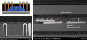 The judges all had different ideas, and it came down to the poll: 3DiS Technologies is the winner. Integrating all building blocks of an RF front-end for 5G applications in a small package and enabling optimal interfacing of the package with antenna array or integrating such antennas inside it (AiP) requires advanced 3D system packaging techniques. These include forming interconnects inside the package, multiple height thru-package-vias, and backside RDL. 3DiS Technologies developed a low-cost wafer-level process that allows the formation of multi-height, high aspect ratio TPVs (10:1) simultaneously with 3D-RDL that interconnects 3D stacked dies inside the package. Not only is this solution is independent of a number of stacked dies and their thicknesses, but it also enables direct 3D integration inside the package cost-effectively. The technology was demonstrated on 3D-IPD devices and 3D RF SiP with stacked dies inside the package.
Research Institute of the Year: CEA-Leti
Runner Up: Fraunhofer ENAS
 Also, a dark horse among the online voters, the judge’s decision prevailed. Leti is paving the way to future high-efficiency systems for high-performance computing with its chiplet-on-interposer concept, as well as its wafer-level integration of thin silicon bare dies within a flexible label. Additionally, ongoing activities in 3D VLSI technology have resulted in the achievement of 1µm pitches in wafer-to-wafer and die-to-wafer stacking using hybrid bonding technology. They are also developing ultra-fine pitch 500 nm hybrid bonding technology. In their CoolCube program, they have proved with a test chip that a 500°C thermal budget for the top layers is acceptable. A multi-project wafer has been recently launched for this monolithic 3D IC solution.
Start-up of the year: Sensry, GmbH
Runner Up: SVXR
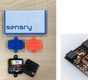 Barely two years old, Sensry GmbH made a great impression on judges and voters alike. The company offers a high level of flexibility for IoT modules, answering the ever-changing customer needs, which is a key to success in this market. Sensry, established in 2018, is working in collaboration with Fraunhofer (development) and GlobalFoundries (production). The company is a lean start-up, driving innovation in a highly insecure environment by implementing the “build-measure-learn” cycle between idea, product, and data. They offer a universal platform for all integrated smart secure sensors. At the heart of the second product generation is a system-on-chip (SoC) developed by Sensry and manufactured by GF in 22nm FDX. The base module hosts the SoC and passives in FOWLP 3D-SiP with TPV interconnect bus to the package backside. The IoT-Module is then customized by heterogeneous integration on package level allowing their customers fast time-to-market. Unlike other solutions, the concept allows access to the latest wafer processing and packaging technologies for fast prototyping and ramp also for SMEs with initially small volumes.
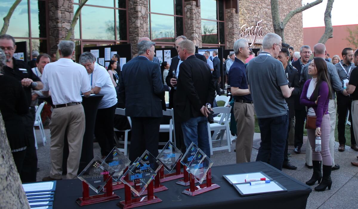
Join us to Celebrate the Winners
We hope all of you will join us in honoring the winners of the 2020 3D InCites Awards in person at the 8th Annual 3D InCites Awards Ceremony and Reception, March 4, 2020, at the WeKoPa Resort and Casino in Fountain Hills, AZ. Festivities begin promptly at 6:30 pm, immediately following the Poster Session at IMAPS Device Packaging Conference 2020. This year’s event will include our third annual STEM fundraiser, during which a local illustrator creates a custom mural onsite that incorporates sponsor logos into an illustration based on a theme. This year’s theme is Integrating Community for a Multi-Dimensional World. Please contact Trine Pierik for details.


