

As IFTLE has been predicting for many years, the baton is once again being passed. In the early days of advanced microelectronics, packaging breakthroughs were developed by integrated device manufacturers like IBM, DEC, NEC, Fujitsu, etc. In the early 2000s, this baton was passed to the OSATS like Amkor, ASE, SPIL, and STATSChipPAC.
As it became more obvious that advanced packaging was going wafer level, it made sense that we would once again see a baton pass to the major lead foundries like TSMC, Intel, and Samsung since they were in the best place to do wafer level packaging development. Since the key packaging conference in the world remains IEEE’s ECTC, one only need to look at what companies are now presenting the key papers at this conference to confirm IFTLEs concept on the transfer of technical superiority.
3D MUST-in-MUST aka 3D-MiM
At the ECTC 20109 in Las Vegas, TSMC showed the world its next-generation packaging, suited to replace standard package-on-package (PoP). The new TSMC acronym, MiM, is quite a mouthful since 3D-MiM stands for 3D MUST-in-MUST, where MUST is short for Multi-stack.
3D-MiM technology utilizes a more simplified architecture that eliminates BGAs between standard PoP packages for system-level performance, power, and form-factor (PPA) purposes. IFTLE predicts that this naming will become very confusing since MiM is already used to describe metal-insulator-metal capacitors. Maybe it will eventually become known as MUST packaging.
Solving the 5G/AI Data Bottleneck?
TSMC notes that in the 5G/artificial intelligence (AI) era, massive data communication has become a bottleneck. Fast data processing requires power computing with low energy consumption. High-speed data communication requires high data bandwidth with low latency. TSMC notes that 3D-MiM fan-out (FO), for logic and memory, was developed for its compact structure, high-density interconnect, improved system performances, and competitive cost. Competitive cost is reportedly achieved by leveraging current infrastructures for yield and capacity.
The modularized memory unit integrates multiple vertically-stacked memory chips by integrated fan-out (InFO) wafer level system integration, with memory I/O pads at one side of the chip. The first 3D-MiM package shown by TSMC (Figure 1) was based on InFO technology. 16 memory chips are integrated into the first two fan-out tiers and a system-on-chip (SoC) is integrated into the third tier. This 3D-MiM package is designed as an alternative solution to the current flip-chip (FC) PoP and FO PoP, currently used in mobile or computing devices but requiring a thinner profile, with high memory capacity and memory bandwidth.
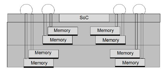
3D-MiM FO represents an alternative solution to a typical mobile PoP, with a thinner profile and shorter wiring between the SoC and the memories. In comparison to the wire-bond memory package, the FO stacked memory module, without BGA connectors and substrate, offers thinner profile and shorter wiring length to reduce the undesired electrical parasitics for power consumption, power/signal integrity, and memory latency.

A larger 3D-MiM FO package was created by integrating 32 memory chips in the first-tier FO, and then integrating eight SoCs in the second-tier FO as shown in Figure 2. This 3D-MiM FO is designed as a low-cost alternative to the current 2.5DIC, for use in 5G/AI-driven high-performance computing (HPC) and server applications requiring high computing performance, memory bandwidth, and low power consumption and latency in applications such as machine learning, and AI training.
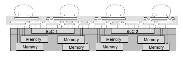
There are no wafer bumps or FC bonding during the 3D-MiM FO integration process to reduce the assembly complexity and avoid the chip-package-interaction (CPI) reliability challenges in FC assembly. Secondly, a much thinner package profile is achieved for the improved form factor, thermal, and electrical performances. Thirdly the tools, materials, and capacity are shared for both mobile and HPC applications to streamline the design rules and shorten product development cycle time for high yield and cost-effectiveness.
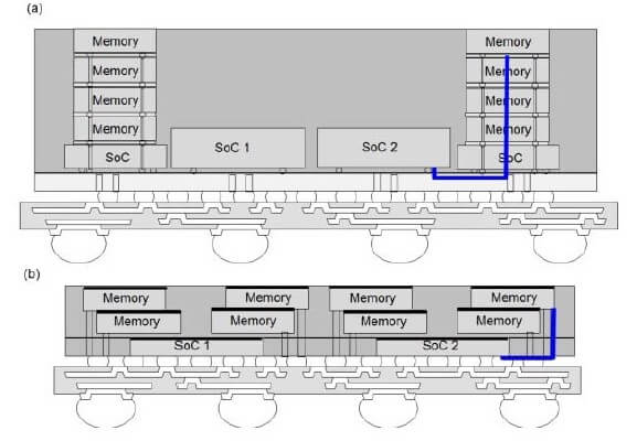
Figure 3 compares the new MiM technology to a 2.5D silicon solution. Unlike a 3D IC high bandwidth memory (HBM) cube, the InFO memory module allows the direct and parallel communication of each memory chip to the computing logic, which helps to improve the memory data bandwidth between SoC and memory. In addition, in 3D-MiM FO, no SERDES controller IC is required, which reduces cost and design/integration complexity. It is observed that, with side-by-side layout, the communication wiring length between SoC and HBM cube of 2.5D IC is longer than that of 3D-MIM fan-out. Aside from that, the footprint and a profile height of 2.5D IC are also greater than those of 3D-MiM fanout.
For all the latest in Advanced packaging stay linked to IFTLE………………………….


