
In this post, we interrupt our regularly scheduled conference review to look at some items that should be of interest to us all.
Is GlobalFoundries (GF) Up for Sale?
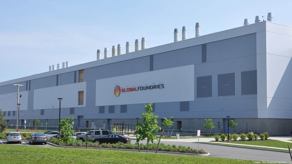
GlobalFoundries is currently the 3rd largest semiconductor foundry supplier with a reported 8.4% market share, just behind TSMC and Samsung. It has five 200 mm wafer fabrication plants in Singapore, one 300 mm plant each in Germany and Singapore, and three plants in the United States, 300mm facilities in Malta, and Hopewell Junction, NY and a 200mm line in Essex Junction, VT.
Rumors are currently rampant that AITC, the subsidiary of the United Arab Emirates Mubadala investment fund that owns 90% of GF are looking to sell off the whole operation. GlobalFoundries has never been profitable. Despite revenue growth, constant equipment upgrades and capital investment have left ATIC with billions of dollars in losses.
Potential acquirers are rumored to be Samsung or SK Hynix. Samsung would reportedly jump to a >23% market share by a GF acquisition. The US would probably block any sale to a Chinese fab such as SMIC.
Similar “For Sale” rumors surfaced in Sept 2018 after GF announced a 5% workforce cut and a termination of its 7nm program, and put all its resources on its 14nm FinFET and FD-SOI processes.
In Dec 2018 GlobalFoundries announced that it had agreed to sell its Fab 3E in Singapore to Vanguard International Semiconductor (VIS).
At the time, CEO Tom Caulfield stated “This transaction is part of our strategy to streamline our global manufacturing footprint and increase our focus in Singapore on technologies where we have clear differentiation such as RF, embedded memory and advanced analog features……..Consolidating our 200mm operations in Singapore into one campus will also help reduce our operating costs.”
When IFTLE first warned that IBM would be selling off all their chip production, many laughed at the “rumors” and said it would never happen, including many, many in DoD circles…you now know that ended!
These GF rumors cannot be seen as good news to the DoD at a time when they are already discussing how to maintain access to state-of-the-art chip technology (both front and back end) in the US.
TSMC – $0.5B Loss Due to Faulty Resist
We all know how complicated the chip fabrication process is, especially at the nodes we are not yet manufacturing. The latest fiasco at TSMC is, therefore, a good reminder for all of us to ensure that specs are being met by incoming materials.
It has been estimated that TSMC had to scrap > 30,000 wafers as a result of using non-spec photoresist. As a result, TSMC will see a $550MM decrease in Q1 2019 revenues (previously announced as $7.4B). Reports are that most of the chips were being produced on the 16/12nm line for MediaTek, HiSilicon, and Nvidia.
TSMC’s photoresist suppliers are reported to be Shin-Etsu, JSR, and Dow Chemical. TSMC’s only public comment was that “TSMC has discovered a shipment of chemical material used in the manufacturing process that deviated from the specification and will impact wafer yield.”
While the foundry declined to identify the source of the defective chemical, the Nikkei Asian Review reported that the bad photoresist probably came from Dow Chemical. I can tell you from my days working in the materials business that if the resist was indeed off-spec, compensation for these losses will be shared by the supplier of the faulty resist, whoever that may be.

BRIDG
When I was an undergraduate at NC State back in the late 1960s Research Triangle Park (RTP) was beginning to grow. It was created in 1959 by state and local governments, nearby universities (Duke, NC State, UNC), and local business interests to serve as a site for high-tech companies to create non-agricultural jobs so university graduates could find jobs in the state. This concept caught on, and over the decades nearly every state has created a similar area. Inside of RTP, in the early 1980s, the state of NC also funded the creation of the Microelectronics Consortium of NC, or, MCNC as it became known. They brought in experts from IBM, Ti and other microelectronic giants of the time and set up a working 1µm line to do precompetitive work. Think of it as a Sematech-type concept.
It is therefore of interest to IFTLE when I discovered that a similar concept was beginning to play out nearly 40 years later in the Orlando, Florida area. In Orlando, they are calling it BRIDG.
The new BRIDG state-of-the-art facility, established as a not-for-profit, industry-friendly public-private partnership, is the anchor of a 500-acre, master-planned technology district owned by Osceola County called NeoCity. It is my understanding that everyone going to Disneyland is, in essence, helping pay for this undertaking. They seek to focus on both R&D and commercialization.
BRIDG has set up a “ boutique microelectronics fabrication facility with 200mm wafer fab capabilities focused on manufacturing development of advanced technologies such as smart sensors, imagers, advanced devices, and 2.5D/3D chip integration” It is the latter that obviously caught my attention. The BRIDG facility provides 109,000 square feet of laboratory and manufacturing space with two cleanrooms, one operating at Class 100 and one at Class 10,000. BRIDG partners will have shared use of capital intensive equipment and infrastructure for semiconductor research and development (R&D), driving down manufacturing process R&D costs.
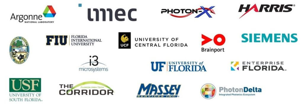
From their website, initial corporate / university partners are shown below.
John Allgair is a 2.5D/3D program manager with background from Motorola, Sematech, and GlobalFoundries. It will be interesting to see what companies join the organization and what their initial efforts focus on. IFTLE will be keeping an eye on them. Their equipment list is detailed here.
For all the latest on advanced packaging stay linked to IFTLE…………………………


