“2.5D and 3D stacking technologies are the only solution that meet the required performance of applications like AI[1] and datacenter as for today”, confirms Mario Ibrahim, Technology & Market Analyst from Yole Développement (Yole). Stacking technologies are used in a variety of hardware, including 3D stacked memory, GPU[2], FPGA[3], and CIS[4], are intended for the high/mid and low-end market segments.
Hardware like HBM and CIS comprise the majority of TSV’s[5] revenue. The overall stacking technologies market will exceed US$5.5 billion in 2023 with a CAGR of 27%, announces Yole it its latest advanced packaging report, 2.5D / 3D TSV & Wafer Level Stacking: Technology & Market Updates report. As for today, the consumer market is the biggest contributor, with over 65% market share. But this, paradoxically, doesn’t mean that consumer is the driver for these technologies. In reality, HPC is the real driver for stacking technologies and will exhibit the fastest growth up to 2023, with market share doubling from 20% in 2018 to 40% in 2023. In terms of packaging revenue, this equates to a more than 6x increase from 2018’s revenue. Consequently, the consumer market’s share will decrease. Other markets like automotive, medical, and industrial will maintain their current market share.
Yole and System Plus Consulting, both part of Yole Group of Companies propose today two dedicated reports that explore the 2.5D heterogeneous and 3D wafer-level stacking technologies. The 2.5D / 3D TSV & Wafer-Level Stacking: Technology & Market Updates report from Yole outlines three stacking technologies, TSV, 3D SoC[6], and hybrid bonding and provides a comprehensive overview of the different market segments including industry trends, market forecasts and technology trends.

In parallel, under its Intel’s EMIB[7] report, System Plus Consulting dives deeply into Intel’s integration know-how with the world’s first on-package CPU[8] and GPU with high bandwidth memory. The reverse engineering & costing company full analyzed the eight generation of Intel core i7 processor. Intel’s processor features a CPU, a discrete GPU and HBM2[9] on the same package. The GPU has a 4GB high bandwidth cache assembled from one 4-Hi HBM2 stack of four DRAM dies, giving almost 200GB/s of bandwidth…
2.5D heterogeneous and 3D wafer-level stacking are clearly reshaping the packaging landscape… System Plus Consulting and Yole invites you to get a deep understanding of the latest technical innovations, the targeted markets and related challenges.
For today’s high-end market segment, the most popular 2.5D and 3D integration technologies on the market are based on TSV for 3D stacked memory, and TSV interposer for heterogeneous stacking.
CoWos[10] technology is already widely used for HPC applications, and new TSV technologies will hit the market in 2019. As an example, Foveros from Intel is based on “active” TSV interposer and 3D SoC technology, with hybrid bonding and TSV interconnections (potentially). Foveros from Intel shows, although TSV is being challenged by non-TSV technologies, companies still have faith in it.
In parallel, Yole’s analysts also underline the emergence of TSV-less technologies in the market. Such innovations can be placed into two groups: “with substrate” and “embedded in substrate”.
 EMIB technology, already commercialized, is part of the embedded-insubstrate group, where the silicon bridge is deep seating in the substrate. Within System Plus Consulting EMIB report, Stéphane Elisabeth, Expert, Cost Analyst at System Plus Consulting underlines Intel’s expertise: “In the past few years, needs for high DRAM bandwidth has led to increasing investments to develop innovative packages. Localized high density interconnects devices between two or more dies has so been investigated. Objective was clearly to provide a higher bandwidth signal in order to open up new opportunities for heterogeneous on-package integration.”…Typical proposed devices are today glass, organic or silicon interposers. And Intel has developed its own approach with EMIB solution, which offers simpler integration.
With-substrate technologies are also used as alternatives to TSV. For example InFO on substrate is widely used in Apple’s processors. Also, RDL[11] interposer technology is currently being developed and will hit the market by 2020. Last but not least, FOCoS[12] was developed and commercialized in 2016, but seems to be lacking orders.
Hybrid bonding can bridge the two main categories (with TSV/without TSV). This technology’s particularity is that it can be simultaneously TSV challenger and teammate. Since 2016 it has been commonly used in smartphones’ CIS, and in the near future it will integrate the high-end market segment for memory and 2.5D as an interconnection solution…
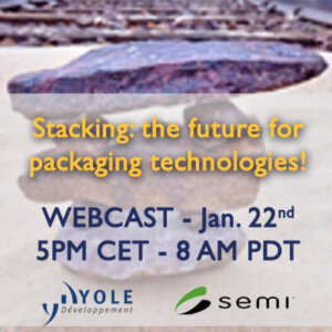 Invited by SEMI for a dedicated advanced packaging webcast last month, Yole proposed a valuable presentation focused on the 3D stacking technologies status and the related market segments. Mario Ibrahim from Yole had the opportunity to point out the technology evolution and market opportunities.
The recorded version is now available: click Stacking: the future for packaging technologies! – Webcast.
[1] AI : Artificial Intelligence

[2] GPU : Graphics Processing Unit
[3] FPGA : Field-Programmable Gate Array
[4] CIS : CMOS Image Sensor
[5] TSV: Through Silicon Via
[6] SoC : System-on-Chip
[7] EMIB: Embedded Multi-Die Interconnect Bridge
[8] CPU : Central Processing Unit
[9] HBM2 : second generation high bandwidth memory
[10] CoWos : Chip-on-Wafer-on-Substrate
[11] RDL: redistribution layer
[12] FOCoS : Fan Out Chip on Substrate
Sources: www.yole.fr – www.systemplus.fr