

Malicious Embedded Chips in our Mother Boards?
Early October brought a report from Bloomberg that I have heard was the top tech story circulating at the DoD and DARPA.
For years, articles about counterfeit chips, and our reliance on Asian-made chips – where they could be modified in ways to pass on information or allow hacks – have worried us. Now…. we’ve got something new to worry about.
According to the Bloomberg report, in 2015, Amazon evaluated a startup, Elemental Technologies, as a potential acquisition for their streaming video service. Elemental made software for compressing massive video files and formatting them for different devices. Its technology helped stream the Olympic Games online, communicate with the International Space Station, and funnel drone footage to the Central Intelligence Agency. Amazon Web Services, AWS, hired a third-party to scrutinize Elemental’s security controls.
The 3rd party discovered that the servers customers installed in AWS’ networks to handle the video compression were assembled by Super Micro Computer, a San Jose CA company that also supplied the server motherboards. Nested on the servers’ motherboards, the testers found a tiny microchip, that wasn’t part of the boards’ original design.
Amazon reported the discovery to U.S. authorities. Elemental’s servers were found in Department of Defense data centers, the CIA’s drone operations, and the onboard networks of Navy warships. Investigators reportedly determined that the chips allowed the attackers to create a stealth doorway into any network that included the altered machines.
Elemental was just one of the hundreds of Super Micro customers. Bloomberg reports that investigators found that the chips had been inserted at factories run by manufacturing subcontractors in China. Bloomberg reports that investigators found that it eventually affected (i.e infected) almost 30 companies, including a major bank, government contractors, and Apple.
The FBI and the Office of the Director of National Intelligence, representing the CIA and NSA, declined to comment. While Apple and Amazon denied the Bloomberg report [link] Bloomberg defended its reporting, indicating that “…the companies’ denials are countered by six current and former senior national security officials, who in conversations that began during the Obama administration and continued under the Trump administration—detailed the discovery of the chips and the government’s investigation.
One of those officials and two people inside AWS provided extensive information on how the attack played out at Elemental and Amazon; the official and one of the insiders also described Amazon’s cooperation with the government investigation. In addition to the three Apple insiders, four of the six U.S. officials confirmed that Apple was a victim. In all, 17 people confirmed the manipulation of Supermicro’s hardware and other elements of the attacks. The sources were granted anonymity because of the sensitive, and classified, nature of the information.”
Certainly, if nothing else, these reports have opened eyes to the issue of not having the capability for packaging and assembly in the US for consumer products, as well as DoD applications.
Leading Edge Chip and Packaging Technology Propels TSMC
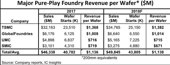
The Oct 12th issue of the McLean report, issued by IC Insights, reveals that the average revenue generated from processed wafers among the big four foundries (TSMC, GlobalFoundries, UMC, and SMIC) is $1,138 in 2018 (200mm-equivalent wafers), which is flat from $1,136 in 2017.
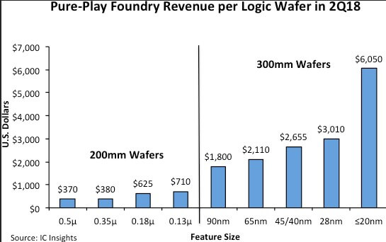
The revenue generated is highly dependent upon the minimum feature size of the IC processing technology. Figure 2 shows the typical 2Q18 revenue per wafer for some of the major technology nodes and wafer sizes produced by pure-play foundries.
In 2Q18, there was more than a 16x difference between the 0.5µ 200mm revenue per wafer ($370) and the ≤20nm 300mm revenue per wafer ($6,050). Even when using revenue per square inch, the difference is dramatic ($7.41 for the 0.5µ technology versus $53.86 for the ≤20nm technology).
Since TSMC gets such a large percentage of its sales from ≤45nm production, its revenue per wafer is expected to increase by a compound annual growth rate (CAGR) of 2% from 2013 through 2018 as compared to a -2% CAGR for the total revenue per wafer average of GlobalFoundries, UMC, and SMIC during this same time period.

IC Insights also concludes that “…there will probably be only three foundries able to offer high-volume leading-edge production over the next five years TSMC, Samsung, and Intel. AS IFTLE has repeated over and over: “The big money is made on the Leading Edge”.
TSMC Market Share Continues to Grow
DigiTimes reports that TSMC had a 56% share of the global pure-play foundry market in the first half of 2018. With TSMC set to be Apple’s exclusive supplier of A-series chips in 2019, they stand a good chance of seeing their global market share top 60% in 2019. TSMC’s 7nm process technology is also expected to obtain orders from AMD, Huawei, MediaTek, Nvidia, and Qualcomm.
TSMC’s InFO wafer-level packaging technology reportedly makes its 7nm process technology more competitive than its counterparts alternatives. With GlobalFoundries putting its 7nm plans on hold and Intel continuing to delay its 10nm production [see IFTLE 395 “And then there were 3…”], TSMC will have few competitors in sub-10nm manufacturing. TSMC reportedly is also ahead of Samsung in the 7nm foundry business as Samsung has reportedly only secured orders from Qualcomm and the Samsung mobile division.
Advanced Chips Need Advanced Packaging
Back in 2014, IFTLE discussed TSMCs ambition of becoming a major player in full back-end ADVANCED Packaging services [ssee IFTLE 190, “TSMC Focus on Packaging…”
In 2016 we examined TSMCs conclusion that in-house packaging was required to spur heightened growth [see IFTLE 283, “Will Packaging make the difference for TSMC”.]
In late September the announcement from TSMC was that they intend to get approval to build a new advanced packaging fab in Chunan Maioli in northern Taiwan. They reported that “Enhancing backend packaging capability will help strengthen our competitiveness in the sub-10nm process by fulfilling orders demanding the foundry’s CoWoS (chip-on-wafer-on-substrate) and integrated fan-out (InFO) wafer-level packaging, and our newly-unveiled system-on-integrated-chips (SoIC) and wafer-on-wafer (WoW) packaging services”.
TSMC understood more than a decade ago that they have a vested interest to ensure that their manufacturing capabilities can continue to increase performance for customers like NVIDIA and AMD, regardless of the fact that Moore’s Law scaling is slowing down. TSMCs major entry into advanced packaging is to ensure their continued financial interests and always has been.
Stacking dies on top of each other through wafer-to-wafer bonding (WoW) using 10µm through silicon vias (TSVs) to interconnect them can improve power efficiency and decrease latency. An operating system would detect a dual wafer GPU stack (for instance) as one chip increasing capacity while using the exact same amount of room as a single card.Cadence has announced that they will support this new WoW technology.
For all the latest in advanced packaging and the IC technology that drives it, stay linked to IFTLE…………….


