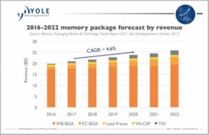
The memory industry is experiencing a strong growth phase: the total memory market is expected to increase at a ~9% CAGR 2016-2022, reaching about US$135 billion by 2022, with DRAM and NAND constituting almost 95% market share. Moreover, a supply-demand mismatch is pushing memory device asking selling price (ASP), resulting in big memory integrated device manufacturers (IDMs) reaping record profits. According to Yole Développement (Yole), the “More than Moore” market research and strategy consulting company, the total 2016 memory packaging market is estimated at about US$20 billion with a 4.6% CAGR until 2022. Therefore, memory devices are using diverse packaging from lead-frame based to through silicon vias (TSVs)
Yole releases today a dedicated report focused on the memory business. The “Memory Packaging Market and Technology” report proposes a deep understanding of the overall market trends of different memory types, related market drivers, and the key applications. This analysis proposes a detailed description of the memory packaging’s evolution and roadmap. The consulting company also proposes to discover the market forecasts of the different memory packaging technologies for the coming years, along with an estimate of future trends.
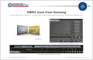
 In parallel, NVIDIA Tesla P100 GPU has been deeply analyzed by System Plus Consulting, a sister company of Yole, in its latest report: NVIDIA Tesla P100 GPU with HMB2. This reverse costing & engineering analysis is showing the technical evolution compared to previous memory generation and highlight the added-value of the packaging part.
What are the latest advanced packaging technology challenges for memory applications? What are the related market issues? Yole Group of Companies, including Yole and System Plus Consulting pursues its investigation towards the memory world and offers you today a deep dive into memories’ world.
“Memory demand is coming from all sectors, particularly from the mobile and computing (mainly servers) markets”, announces Santosh Kumar, Senior Technology & Market Research Analyst at Yole.
On average, DRAM memory capacity per smartphone will rise more than threefold, reaching around 6GB by 2022, while NAND capacity per smartphone will increase more than fivefold, reaching more than150GB by 2022. For servers, DRAM capacity per unit will increase to a whopping more than 0.5TB by 2022 and NAND capacity per SSD for the enterprise market will reach more than 5TB by 2022. Growth in these markets is fueled by applications such as deep learning, data centers, networking, augmented reality and virtual reality (AR/VR), and autonomous driving.
In parallel, the automotive market which generally use low-MB memory will see the adoption of DRAM memory led by emerging trend of autonomous driving and in-vehicle infotainment. Also, the NOR flash memory market is resurgent and expected to grow at an impressive 16% CAGR, attaining about US$4.4 billion by 2022 due to its application in new areas like AMOLED display, touch display driver ICs, and the industrial internet of things (IoT).
 On the supply side, player consolidation coupled with the difficulty in migrating to advanced nodes due to technical challenges, along with higher investment and migration from 2D to 3D NAND, has caused a shortfall in DRAM and NAND flash supply. DRAM players want to retain high ASP and profitability to justify their huge capex investment for advanced node migration, and as such are not inclined to increase capacity.
There are many different memory device packaging options, implying a wide range of packaging technologies ranging from low pin-count SOP[10] packages to high pin-count TSV options, all depending on product requirements like density, performance, and cost.
“We have identified five core memory device packaging platforms: viz lead frame, wire-bond BGA, flip-chip BGA, WLCSP, and TSV,” asserts Santosh Kumar from Yole. “Each one includes many variations, along with different terminology. Ultimately, the total memory package market is expected to reach almost US$25 billion by 2022.”
In 2016, wire-bond BGA accounted for more than 80% of the packaging market in dollar terms. Also in 2016, flip-chip began making inroads in DRAM memory packaging, and is expected to grow at about 20% CAGR over the next five years, accounting for more than 10% of the total memory packaging market. Increased adoption in the DRAM PC/server segment, fueled by high bandwidth requirements, drives flip-chip growth. Samsung has already converted more than 90% of its DRAM packaging line, SK Hynix has also started converting, and other players will begin adopting flip-chip in the future. In fact, all DDR5 memory for PC/servers will eventually use flip-chip.
Spurred on by high bandwidth and memory chips’ low latency demands for high-performance computing in various applications, TSV is being employed in high-bandwidth memory devices.
“As an example, HBM2 from Samsung and developed for NVIDIA Tesla P100 GPU greatly increases memory capacity and bandwidth over the previous generation”, explains Romain Fraux, System Plus Consulting’s CTO. And he adds: “The single package 55 mm x 55 mm 12-layer BGA package includes more than 3,500 mm² of silicon area. A 3D-assembly process yields HBM2 stacks composed of four 1 GB DRAM memory dies and one buffer die, connected with via-middle TSV and micro-bumps…” (Press release).
The 2016 TSV market was only less than 1% of the total memory market, but this will grow to more than 30% CAGR, reaching about 8% of memory packaging in dollar terms by 2022. Also, WLSCP packaging is used in NOR flash and niche memory devices and is expected to grow at a more than10% CAGR, but in terms of value will remain only less than 1% of the market by 2022.
For mobile applications, memory packaging will mostly remain on the wire-bond BGA platform. However, it will soon begin moving towards the multi-chip package (ePoP for example) for high-end smartphones. NAND flash devices’ main requirement is high storage density at low cost. NAND are stacked using wire bonding in order to provide high density in a single package.
NAND flash packaging will remain in wire bond BGA form and will not migrate to flip-chip. However, Toshiba will start using TSV packaging in NAND devices to increase data transfer rate for high-end applications. After Toshiba, Yole believes Samsung and SKHynix will bring TSV packaged NAND devices to market.
The market research and strategy consulting company Yole, will attend SEMICON Europa (Nov. 14-17 – Munich, Germany) and will make some presentations focused on its activities (SEMICON Europa agenda). One of them titled “Advanced Packaging: A very dynamic ecosystem!” will deliver the technical challenges and market issues with a dedicated part on the memory business. Yole’s speaker will be Andrej Ivankovic, Market & Technology Analyst, Advanced Packaging & Manufacturing. Save the date in your agenda and meet Yole’s team on booth B1-1434.
A description of the Advanced Packaging for Memories report including table of content, list of companies mentioned in the report and more is detailed on i-micronews.com, advanced packaging reports.
Source: www.yole.fr


