
Consider for a moment that the ultimate goal of 3D integration is not to achieve high volume manufacturing (HVM) in high bandwidth memory and logic applications for mobile devices, but rather to be an enabler for heterogeneous integration of disparate technologies for everything from medical and automotive applications to industrial sensing, military and the Internet of Things (IoT)? Would that create a viable and successful market? What if it offered small- and medium-size semiconductor manufacturing companies the opportunity to grow and prosper alongside the big four (TSMC, Intel, Samsung, and Global Foundries); maybe not topping the charts, but providing much needed innovation in many market sectors requiring innovations in computing. Would that be enough to say that investment in 3D integration is a worthwhile endeavor? If the answer is yes, than I think its safe to say that 3D has indeed arrived and is quite real for many.
At SEMICON West 2014, I talked with some of the usual suspects from R&D, manufacturing and suppliers, and while some are still holding out for that HVM return on investment, others see the rich opportunity in a myriad of low- to mid-volume applications. Indeed, several of the research centers have shifted focus from technology development to system level integration; grasping that opportunity and putting 3D to work in real applications.
Klaus-Dieter Lang, director, Fraunhofer IZM; the arm of the microelectronics division of Fraunhofer Institute that is responsible for assembly, packaging and hardware reliability and micro-integration; explained how philosophies have evolved over the years at the Berlin-based institute. In the early days (the 90’s and early 2000s) the focus was on the development of specific standard components based on wire bond structures that then shifted to flip chip technology, and then to system integration.
“Now, the system has to be optimized and merged with the application environment,” he explained, citing the work IZM is doing in smart textile development as an example. It’s very difficult to standardize this. He predicts that due to need to optimize packaging and assembly solutions to specific applications, the volume is decreasing. He says that due to technology shifts like the IoT and cyber-physical systems, stand-alone components will disappear. “We need new approaches for packaging and assembly,” he said. “One is 3D integration at the wafer level, the second is panelized packaging from the substrates side, which will put this into functionality of the final product.”
To adapt to these changing needs, he’s organized the institute to integrate design groups, reliability experts and process engineers as part of these lines. “Its organized better. We’re doing what the industry should be doing,” he said. “If you want to do system-in-package (SiP) or wafer-level-package (WLP) with high complexity, you have to change your way of doing things that requires collaboration between the design community and manufacturing community.”
We talked more specifically about the Cluster for 3D Integration, a collaboration of several Fraunhofer Institutes (IZM-ASSID, ENAS, IKTS, IIS-EAS, and IPMS), each of which bring different core competencies to the table; and together deliver a holistic approach to the design, development, and implementation of 3D heterogeneous systems for its industrial partners. With 3D integration, explained Dieter, it takes effort to determine where the advantage is to use it, so they brought together partners inside of Fraunhofer to work on this.
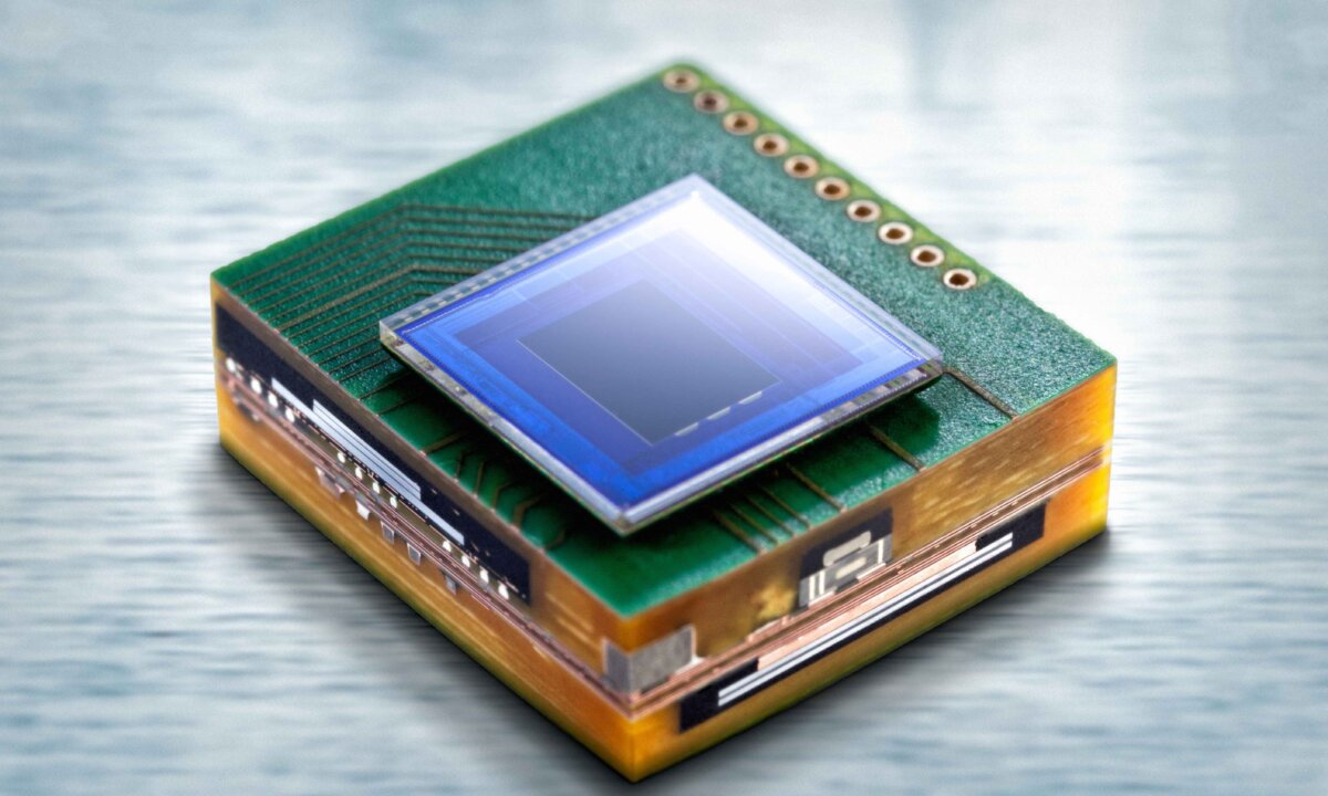
“The importance of packaging will only increase in the future with complex high frequency systems,” he noted. We need new approaches and new materials. He also said he believes that fan-out wafer level packaging (FOWLP) and 3D will exist side by side. At Fraunhofer, they’re working on system integration technology for such applications as tire pressure sensor systems, environmental sensing, and a five megapixel high-performance wafer level camera (feature image).
Another research institute focused on low-volume applications for 2.5D and 3D integration that shares a similar vision to Fraunhofer IZM is Research Triangle Institute (RTI) located in Raleigh-Durham, North Carolina. In fact the two organizations have collaborated on jointly developed projects, and together won the ECTC 2011 Best Session Paper titled “Characterization and Failure Analysis of TSV Interconnects: From Non-Destructive Defect Localization to Material Analysis with Nanometer Resolution” by Michael Krause, Frank Altmann, Christian Schmidt, and Matthias Petzold (Fraunhofer IZM); and Dean Malta and Dorota Temple (RTI International).

Alan Huffman, WLP Research Engineer & Program Manager, talked to me about RTI’s low profile in the 3D space, and brought me up to speed on the organization’s back-story. It began as Microelectronics Center of North Carolina (MCNC) as a state-supported R&D center to support local universities before it became a part of RTI International, a globally recognized research institute that provides a broad spectrum of research and technical services in areas such as health and pharmaceuticals, education and training, surveys and statistics, advanced technology, international development, economic and social policy, energy and the environment, and laboratory testing and chemical analysis.
While MCNC started out as a research center for CMOS fabrication, recapitalizing it to keep up with the latest design rules and lithography tools was expensive for a state agency, explained Huffman. So in the 90’s the focus shifted to other applications and technologies like MEMS and flip chip that would draw DARPA funding. Research focused on stretching the boundaries of flip chip to develop high density bump technologies; applying it to such devices as multi chip modules (MCM) for particle accelerators, like the Hadron Collider in Cern, Swizterland. Huffman said the organization found a niche in providing small volume access to advanced capabilities. They also worked on bringing materials characterization into the WLP environment.
MCNC sold its research division “relatively quietly” to RTI in 2005, said Huffman. The focus is on interconnect development that is performance driven, not volume driven. The fit for developing 3D integration technologies was a natural because they already knew how to micro-machine silicon, and had developed processes for through-hole etching, said Huffman. As with its flip chip work,they work on early-stage development of 2.5D and 3D processes. The goal at this “growth stage” is generating a 3D TSV or interposer wafer, implement new tools, and expand throughput in the area. (You can read more about their approach to 3D in an interview with Dean Malta at ECTC 2014.)
Organizations like Fraunhofer IZM and RTI have been critical to the development of 3D integration technologies, and success for them is not dependent on HVM in mobile devices. They see plenty of opportunity for 3D in applications like defense, security, high performance computing, medical electronics, and the IoT. One example of 3D success in this type of application is the winner of the 2014 3D InCites Award Device Category. SORIN Group won for its 3D IC module for active medical implant, a collaborative development of the E-BRAINS consortium including Fraunhofer IIS/EAS, 3D-PLUS and SORIN Group. The device targets pacemaker applications, a market that hit $4.3B in revenue in 2012. Put several these markets together where 3D ICs enable next-generation devices, and it seems to me you’ll get to big enough volume to justify its existence. I’ve said it before and I’ll say it again: 3D doesn’t have to be HVM to be real. ~ F.v.T.


Francoise, great companion piece to your earlier one on HVM and 3D IC. BTW, just what is the definition of HVM? Agilent has shipped billions of FBAR filters with TSV technology without it being called HVM, or at least not being called it by CMOS silicon people.
Hi Paul,
Remember that TSV alone is not synonymous with 3D. Even though TSVs have been used in volume for FBAR filters, if its not a 3D architecture, it just means TSVs have been used in volume. Many will argue that although backside TSVs have been used in volume in CMOS Image Sensors, it doesn’t mean CIS is a 3D device. Next generation CIS with backside illumination in a 3D stack (with the IC stacked rather than next to the sensor) is the first true 3D IC configuration of CIS.
I think HVM means different things to different people. But for most, it seems to mean when 3D ICs are mainstream in the mobile market.
Intel’s decision to try out Micron’s HMC at the high end ( Xeon Phi modules to build Crays ) next year is logical and shows sound engineering judgment absent among the Bloggers & Boosters of TSV based 3-d stacks who for a few years had been predicting their imminent use in every SmartPhone !
But the fact that Power Point engineers and Bloggers w/o the benefit of any Physics got a bit too excited about TSV based 3-d homogenous stacks, does not necessarily mean that TSVs are not worthy of HVM.
Certain camera modules ( heterogeneous ) for Mobile phones use TSVs and have been in HVM for at least a year. But in these Modules the TSVs are only at the die periphery – none in the active area, and there is little trapped heat or stress in the stack .
Dev,
Micron is very careful to point out that although the stacked memory used in Intel’s Xeon Phi is fundamentally based on HMC, it is NOT HMC, and it is exclusive to Intel. Additionally, HMC was developed by a consortium to solve the memory bandwidth problem for CPUs and GPUS and has not claimed to target the smartphone market. Rather it has always been targeted for high performance computing and ultimately consumer technologies like tablets and graphics cards.
With the exception of some monolithic 3D IC technologies and something referred to as “superPoP with magic chips”, many of the viable 3D IC devices using TSVs have moved beyond power point engineering to test vehicles, customer samples, and actual products being produced in low volume. I’m pretty confident that 3D is here and will hit HVM solidly in the next few years.
The question is whether these niche applications can together support R&D and drive standardization of design rules and processes.
The general belief is that, similar to Flip Chip adoption, these low-volume, high end computing and niche applications will ultimately lead to high volume adoption as the processes are optimized and cost is reduced.
ACCESS (Advanced Chip Carriers & E-Substrate Solution) is with unique pillar technology and it can facilitate “panelized packaging in substrate-site”.