


Two years ago, I visited to Fraunhofer IZM-ASSID, located in Dresden, Germany; to see first-hand what this particular arm of Fraunhofer Gesellschaft was all about. Juergen Wolf, head of IZM-ASSID, gave me the grand tour of the 300mm cleanroom and explained the organization’s focus on developing Cu TSV technologies in 300mm wafers for both 2.5D interposer and 3D IC applications. For the past year, when I have met up with Wolf at various industry events, he’s been talking about the Cluster for 3D Integration, a collaboration of several Fraunhofer Institutes (IZM-ASSID, ENAS, IKTS, ,IIS-EAS, and IPMS), each of which bring different core competencies to the table; and together deliver a holistic approach to the design, development, and implementation of 3D heterogeneous systems for its industrial partners. At the invitation of Wolf, I returned for a second visit to Fraunhofer IZM-ASSID to meet his Fraunhofer colleagues and learn more about how this cluster came to be, and what its goals are.
In addition to Wolf, my Fraunhofer Society welcoming committee included Stefan Schulz, head of the back-end-of-line department for Fraunhofer Institute for Electronic Nano Systems (ENAS); Dr. Michael Galetzka, head of business development for the Fraunhofer Institute for Integrated Circuits (IIS), Design Automation Division (EAS); Prof. Dr. Ehrenfried Zschech, division director of nanoanalysis and testing systems for the Fraunhofer Institute for Ceramic Technologies and Systems (IKTS) and Peter Schneider, Division Director for Fraunhofer IIS-EAS, who joined the party in progress. (Blogger’s note to readers: If you find these acronyms confusing, its because they represent the German words, not English.)
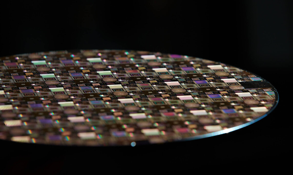
As previously mentioned, IZM-ASSID is focused on the technology; including 3D wafer level integration technologies and all the technologies required to support it. It offers a 3D technology line for low volume prototyping and manufacturing, material and equipment evaluation. “Beside the large foundries, many of our activities are driven by small and medium -size industry partners who don’t have the capability of a complete process line to build 3D systems,” explained Wolf.

While Fraunhofer ENAS specializes in integration of functional components for smart systems, Schulz explained that the focus is on integration of MEMS devices and electronics for data acquisition and sensor control e.g. for inertial sensor systems (Figure 1.) The work of the 3D and system integration team at ENAS is to improve on the interconnect systems, as well as contributing to process and technology development and thermo-mechanical reliability related tasks. “We build complete systems integrating sensors, wireless transmitters, and controllers together,” he explained.
Formerly the Fraunhofer Institute for Non-destructive Testing, (IZFP); it was recently integrated into Fraunhofer IKTS to strengthen its services and research co-operations for the diagnosis of materials as well as components, nanoanalysis and sensorics, etc. As part of the cluster for 3D, explained Zschech, efforts will be focused on materials characterization, process control and quality control for 3D integrated systems. In addition, reliability-limiting degradation mechanisms in 3D-stacked chips are studied. The IKTS also works in collaboration with the Dresden Center for Nanoanalysis. (My visit included a tour of the analytics lab, which was quite impressive. Details to follow.)
Fraunhofer IIS-EAS is the division for electronic design automation. Galetzka explained that this group works on all aspects of design automation, including developing design methodologies, design and modeling tools for complete system design. “We have developed our own tool for design space exploration for 3D integration, and also for 3D floor planning. Our goal is to fill in the gaps in the design process,” he explained. IIS-EAS offers design services to its customers. “If a customer wants a high performance system, like a processor with a fast memory, we explore the possible design options to meet the requirements. If 3D integration turns out to be the best solution we also do the thermal analysis and the floor planning and design the interposer,” said Galetzka. “And we have the methodologies and tools to address all the problems.”
All of these Fraunhofer Institutes have been contributing their competencies individually for the commercialization of 3D integration for sometime, and often had worked together on various projects. They became a formally organized group about a year ago, in an effort to identify and avoid overlaps, and also to provide one access point to coordinate activities inside the group.
Here’s how it works: when an industrial partner approaches any one of the group with a project, they hold a customer-specific workshop to determine the customer needs and then develop a business model to address the needs within the cluster. They deliver a statement of work and proposal to the customer, who then reviews and defines the project further. Then there is alignment between the institutes to determine what part each partner contributes. According to Galetzka, the point of entry is for example, IIS, as the customer comes with a design problem and the solution turns out to be a 3D design. Another point of entry could be IZM-ASSID when the project is technical/technological driven, says Wolf.
“You can be certain a system designer doesn’t know the advantages of 3D when he designs a traditional system,” he said. “We bring new ideas to the customer and have to know the overall perspective. What is the next step after the interposer for the assembled die? What are the conditions? Who is doing the assembly? We can identify the critical steps if we have an overall view from the beginning.”

Wolf explained that the team defines a goal with one model, and decides what technology approach is needed, and from there develop the design guidelines, material aspects, simulation and reliability. “We build the model on 3D systems, test the sample, compare the results, and build up the model to be more precise,” he explained. They take a step-by-step approach to identify points of decision and work together to find a workable solution. When it comes to integrating a MEMS device, “The customer doesn’t know how the impact of a 3D technology will affect the device. It’s very important to give knowledge for estimating what the impact is on the device and give a process flow,” explained Schulz.
Ultimately, explained Wolf, the role of the Fraunhofer 3D Cluster is to look at the system from all perspectives from functionality, design, technology, performance and reliability and provide an integrated solution as a system integrator. In other words to use the complete value chain available in the cluster to serve the customer for a successful 3D solution.
The Tour
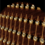
Rather than the usual cleanroom tour (although I did get a window tour of the MEMS 200mm fab), I was treated to a demo of some state-of-the-art characterization tools in the analytics lab, located near IZM-ASSID at the IKTS Dresden location, including a focused ion beam (FIB) microscope that can micro-machine samples in the nano-scale to characterize 3D structures; a transmission electron microscope (TEM) that can achieve atomic-level resolution; and a nano X-ray tomography system for detecting voids and defects in through silicon vias (TSVs) and micro bumps. Fast preparation of TSV samples was part of a joint development project (JDP) with Carl Zeiss Microscopy for the Auriga Laser tool, explained Ruediger Rosenkranz.
While I looked on, the technician, Yvonne Standke manipulated a sharp needle to lift out a sample measuring 100nm (1000th the diameter of a human hair) that was transferred then to a TEM grid to characterize materials used for isolation, barrier and fill of the TSV. Another partner project that requires use of the TEM is determining mechanical stress in silicon based depending on the distance of the transistor from the TSV. “Measuring this is challenging,” explained Zschech, “If you can determine the strain in the silicon you are able to validate physical models used for multi-scale simulation, to optimize the position of the transistors in relation to the TSVs and to reduce the so-called “keep-out-zone” areas,” he explained.
manufactured at IZM-ASSID, studied at TU Dresden/DCN).
The last tools I saw in action were the XCT tools: a self-built micro X-ray tomography tool that is used for nondestructive characterization e. g. for packaged products with micron resolution. Zschech explained that Fraunhofer IKTS works closely together with the Dresden Center for Nanoanalysis at TU Dresden, where a new Carl Zeiss sub-micron XCT tool was installed. The high-resolution nano X-ray tomography system with 50nm resolution is used to detect voids in TSVs, characterizing filling failures. The major focus of this work at IKTS for the 3D Integration Cluster is on the analytical techniques for process development and reliability engineering.
For some time, the industry has called for a collaborative ecosystem for the realization of 3D integration technologies. It is clear tome from my visit that Fraunhofer’s 3D Integration Cluster is heeding that call, and providing the necessary elements to offer a holistic approach to development and manufacturing 3D integrated systems in Europe. I look forward future progress reports as the concept matures and takes hold. ~ F.v.T.


