
The Friday 3D Integration Workshop at DATE 2014 once again found me among friends, as an intimate group of about 30 gathered to spend a day sharing knowledge gained since last year’s workshop. My key take-away for the day was how to achieve reliability and robustness. Jürgen Wolf, director of the Fraunhofer IZM-ASSID 3D integration program stepped in as keynote speaker to replace Yole Développment’s Rozalia Beica, who was unable to attend, and as such we were treated to a great combination of Wolf’s slides seasoned with a number of Yole’s. It was interesting to get Wolf’s perspective on Yole’s market research. Invited speaker, Maaike Talko, SINTEF, brought the gathering up-to-date on EU funded work for integration of bioMEMS and ICs using 3D integration technologies, and the benefits we can gain from that work. There were some interesting technology updates, particularly in the area of thermal modeling, and we had a lively, interactive panel discussion addressing the question of whether slow standardization and CAD tool development are hindering the progresmm of 3D IC design and integration. Wolf set the tone, talking about global social megatrends we’re facing. “How do we find a technical answer to manage the changes of social society as the world becomes more and more digital? We need to find technical solutions for managing data.” He noted, adding that Industry 4.0 is a keyword for industrialization, as is “cyber-physical systems” aka “The Internet of Things.” Fraunhofer IZM-ASSID has trademarked a new heterogeneous device, the eGrain™, comprising four technology blocks: sensing (MEMS, sensors, actuators); data processing (IC, memory, MPU, passives); acting (power management) and communication (transmission of data via RF devices. Adding yet another acronym to the ever-growing advanced packaging lexicon, Wolf says this eGrain will integrate system on chip (SoC) advanced CMOS with disparate technologies using system in package (SiP) approaches to create a 3D SiP. “Today, we already have a good technical baseline for implementing 3D technologies.” he noted. He talked about the Fraunhofer vision for interposer generations (G2-G5), converting ultimately into an integrated active multifunctional packaged device that provides not only TSV and multilayer redistribution (RDL) on both side, but also features integrated passives; embedded actives and/or MEMS; integrated optical & electrical interconnects, and active cooling. Wolf has dubbed this an “integrated interposer wafer level package” or I2WLP. (Yes, ANOTHER acronym! Will the madness ever stop?)
From Yole, he shared a slide (Figure 1) predicting that 3D technologies are expected to have high growth, reaching 9.2M wafers by 2017. While Yole tends to be consistently overly optimistic in its predictions, what I found most interesting in this slide is that while approximately 61% of the market will be mobile phones, tablets and laptops, the remaining 39% provides the opportunity for Europe to succeed in its vision of Horizon 20/20 – reclaiming 20% of the semiconductor manufacturing market by 2020. 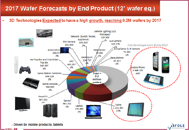
Talko talked of Horizon 2020 during her presentation, providing an update of EU funded projects SINTEF has been involved with, including e-CUBE and e-BRAINs. The combined goal of all these programs is to answer the challenges of health, well-being, and food security through integrated technologies. With the Horizon 2020 initiative in particular, she says there is a great emphasis that work in research institutes must transform into work for others. So it’s not sufficient to develop only proof of concept, researchers now have to ensure these devices can be fabricated in an industrial environment. “This is not the first thing you usually think about in a university environment,” she noted. For this reason, there is new emphasis on ensuring robustness and reliability from the start of development. Process control and designs that achieve repeatable results are now the main focus. The design needs to cope with natural variations. “If you can understand failure mechanisms from the inner part of each chip, there is a better chance for the whole system to be reliable,” she said, adding that now, there is emphasis on studying each part being put together for reliability and robustness, and take care of the interfaces as well. Lastly, as we are making things that at some point will be disposable, she said care must be taken to develop “compostable electronics.” Much of the work Talko has focused on recently involves the bridge between biosensors and silicon devices to create personalized health sensors for early treatment and detection of heath conditions, with the ultimate goal of keeping people out of the hospital. She presented a number of early-phase projects such as devices to test for glucose, glutamate, DNA sequences and pH; and a pathogen-specific biomolecular sensor. With all this focus on reliability and robustness from design, I would be remiss if I didn’t point out several other presentations that reported findings and offered solutions to the thermal modeling issues. Kristof Croes, who works in 3D reliability research at imec, reported on various projects he’s worked on to address reliability challenges for 3D stacked ICs (3D SIC) including the through silicon via (TSV) and its environment; back-end-of line (BEOL) reliability challenges with Cu and dielectrics; Cu diffusion, TSV presence and proximity. So far, much of the work he’s done has turned up favorable results. “3D reliability is a challenge of 3D integration, but there has been no show-stopping phenomena so far,” he said. Other concerns that require attention in addition to reliability, he said, include chip package interaction (CPI), and thermal behavior. As luck would have it, there were two presentations that talked about thermal challenges. Unfortunately where there are no reliability show-stoppers, Frank Altmann, of Fraunhofer IWM in Halle, Germany, performed advanced failure analysis on 3D packages and has determined that thermal issues may indeed be a showstopper for 3D, and have to be addressed at all levels, including the fab. He said several technical parameters can be optimized to address thermal problems in the fab, and during assembly and test. “We have performed accurate assessments through coupled simulations and by taking in-situ measurements,” he explained. “Silicon is driven towards thinner dimensions to improve TSV density and performance, which worsens the thermal problem in 3D stacks.” On the bright side of this, Pascal Vivet, also of Leti, updated me on the collaboration with Docea Power to develop a thermal modeling tool to do system-level exploration of thermal effects before the system is built. “We don’t want to use tools at the package level because working at the system level allows us to decide early on what do to with a complex system, and we can refine the model with more accuracy,” he explained. The tools are used for co-simulation between the virtual platform and hardware to develop both a power model and a thermal model. Thermal mitigation can be done in the software to evaluate what’s happening in the hardware, he explained. He was happy to report that the work they’ve done with Docea has been proven on a 3D wide I/O memory on 65nm logic design. Using heaters and thermal sensors, they can generate heat on demand and do a fast thermal simulation that correlates with silicon measurements. “It’s a nice characterization tool and is used to validate the thermal model,” said Vivet. The best part is that the tool works, and is commercially available. (A thermal modeling tool has been high on Jan Vardaman’s wish list. Let’s hope that this raises her report card grade on the thermal challenges.) The 3D panel was so lively, that it really deserves a blog post all its own, so that’s what I’m going to do. Be on the look out for it. ~ F.v.T.


