
What is today’s biggest threat to continued growth in the semiconductor industry?
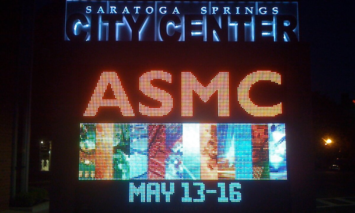
Subramani Kengeri, Vice President, Advanced Technology Architecture, GLOBALFOUNDRIES, opening the 24th annual SEMI Advanced Semiconductor Manufacturing Conference in Saratoga Springs, NY, asked just that question in his keynote address. (Asked it twice, actually; once at the beginning of his provocative talk, and once again at the end, looking to crowdsource the answer.)
You have two choices: Is the biggest threat to semiconductor industry growth the one posed by fundamental technology scaling limits, or is it the threat posed by business fundamentals/economic realities? (And here at 3D InCites we want to know “Just how does 3D IC fit in to all this?”)

Using System-on-Chip (SoC) products as his representative example, Kengeri examined the technology limitations facing advanced SoC designs as GloFo and its customers work to realize the value of technology scaling. He also looked at the economic realities — the techno-economics — of achieving rapid time-to-volume (TTV) on bleeding-edge technologies in advanced semiconductor wafer fabs (like GloFo’s nearby Fab 8 in Malta, NY) to achieve a healthy ROI from the massive capital investments required to build and outfit a fab at the 28nm ($4.85B) and 20nm ($6.7B) process nodes.
Basically, from Kengeri’s wafer foundry perspective, ROI for these advanced process nodes looks to be delayed as a result of the increased investment required in fab gear, process development, and chip design costs (covering the “I” side), and also because achieving TTV in high volume manufacturing (HVM) now takes longer and longer compared with historical norms, delaying revenue and impacting positive cash flow (the “R” side).
And why is that? According to Kengeri, these days achieving productive TTV can be slower due to the higher level of integration inherent in the advanced SoC space. There are new yield ramp challenges as disparate functionalities (applications processors, GPS units, NFC Controllers, other IP) are integrated into new single-SoC designs.
GloFo sees 3D packaging as one of today’s key new techno-economic challenges. On the technology side, 3D packaging is clearly something new, but on the economic side it may be that some of the other, more difficult (EUV anyone?), techno-economic challenges facing the industry means that SoC suppliers are looking to 3D IC packaging schemes as a way to rise above the money pit being dug in the advanced lithography module.
Maybe it’s time to via?
Oh, and on the crowdsourced answer to whether it’s technology limitations, or economic realities, that are most likely to hold back continued semiconductor industry progress, the 300+ ASMC 2013 attendees overwhelmingly voted “Economic Realities.” I think Kengeri was leading us on toward that conclusion anyway from the way he positioned his talk, but even he had to smile at the lopsidedness of the vote.
In the spirit of ASMC being a venue for industry professionals to network, learn and share knowledge on new and best-method semiconductor manufacturing practices and concepts, GLOBALFOUNDRIES went on to provide a detailed 3D IC tutorial on ASMC Day 3 (after hosting a fabulous “Welcome to Saratoga Reception” at Fab 8 the evening before – thank you GloFo!).
The tutorial, given by Sarasvathi Thangaraju, from GLOBALFOUNDRIES’ Package Technology and Integration Group, had the practical title of Implementation of an Industry Compliant Aspect Ratio 10, Via Middle TSV.
 Thangaraju told us everything we need to know (almost) about the via middle TSV process (aka: Middle of Line) and packaging flow GloFo developed in order to mate wide I/O DRAM, or other core components (per Kengeri these core components will come down to be only DRAM, NAND Flash, miscellaneous peripherals, or MEMS; everything else integrates), with SoC devices using 3D IC packaging.
Why via middle TSV? From the tutorial, we heard that MOL TSV is easier than via last (aka via late; Back End of Line) because all the BEOL optimization that’s already part of the standard foundry process flow can basically port over to the via middle process undisturbed. And since half the process steps these days in SoC fabrication seem to be BEOL metallization steps, that’s a huge advantage.
Highlights for me from Thangarju’s tutorial included learning just how often (6 time by my count) GloFo makes in-line film stress measurements during the TSV process module. (This is good news if you are an in-line film stress metrology tool maker.)
The TSV etch itself seems to be pretty well understood by GloFo, with some important notes being that etch profile is critical to post-etch CMP processing (stress raising its head here if the etch profile’s not right); that there are effective ways to remove the characteristic Bosch process scallops post etch (reference given here to a paper by Fujitsu about TSV scallops and leakage currents); and that the post-etch wet clean implemented by GloFo both removes polymer residue left from the TSV etch and creates hydrophilic surface conditions, useful for some of the metal deposition steps that follow.
(Being a via middle process, the TSV etch isn’t really through silicon, it’s blind-stop-in-silicon, but you knew that already, right?)
A 400° – 420°C pre-CMP anneal after copper ECP eliminates via fill copper expansion, which is a good thing (stress, extrusion).

Future plans for GloFo include taking the current 6µm x 55µm vias down to 3µm diameter vias to reduce the real estate devoted to Keep Out Zones. Since deleterious effects (primarily via-induced stress) created by TSV structures scale proportionally with the via diameter squared, reliably made, smaller diameter vias are the way to go. Smaller KOZ you know.
ASMC 2013 dedicated a complete session, Session 3, to 3D/TSV Technology this year, and I now know that Georgia Tech (Paragkumar Thadesar, Novel Photodefined Polymer-Clad Through-Silicon Via Technology) has a good handle on obtaining optical endpoints from Bosch Process etching of silicon in TSV applications; that SEMATECH (Stephen Olson, Challenges in Thin Wafer Handling and Processing) likes mechanical peel debonding for temporary bond-debond; and that Tohoku University (Mariappan Murugesan, Mechanical Characteristics of Thin Dies/Wafers in Three Dimensional Large-Scale Integrated Systems) is paying attention to the question of “Just how strong are thinned silicon wafers / thinned silicon dies, particularly if you’ve just poked holes in them with your TSV process?”
Riffing on both the SEMATECH and Tohoku University talks, Professor James Lu, RPI, asked the great question “Why can’t we just get rid of handling thin wafers at all?” (James, you seem to know the answer already – perhaps you’ll share something with 3D InCites sometime soon? Kudos to you also for the paper by you and Huanyu He, and your IBM colleagues, on TSV Density on 3D Power Delivery with High Aspect Ratio TSVs.)
On the 3D metrology front, IMEC (Sandip Handler, Metrology and Inspection Challenges for Manufacturing 3D Stacked ICs) has in their metrology quiver a scale for measuring changes in wafer mass and thereby determining TSV etch depths in their MOL TSV process; a Scanning Acoustic Microscope for in-line copper void inspection, and for identifying wafer-to-wafer bonding defects; and an optical measurement tool for precisely measuring true wafer thicknesses prior to TSV reveal.
About X-ray microscopy, the conference was of mixed opinions. IMEC said X-ray inspection of TSV features needs to be improved from its current state, conventional wisdom being that its current state is useful, albeit slow, as Yuri Sylvester, Xradia (3D X-Ray Microscopy: A Non-Destructive High Resolution Imaging Technology That Replaces Physical Cross-Sectioning for 3D IC Packaging) reminded us, before turning around and letting us know some of the practical use cases Xradia can point to for X-ray metrology in 3D IC packaging applications.
There’s still a way to go before X-ray microscopy will be a useful technique for in-line monitoring. Issues needing to be addressed include throughput, and automatic sample handling.
One notable poster by Corning Incorporated (Glass Substrates for Carrier and Interposer Applications and Associated Metrology Solutions, presented by Linh Au), covered some of the important potential advantages of using glass substrates instead of silicon for 2.5D and 3D IC. Corning proposes these advantages are first and foremost lower cost (as a result of using large glass panels, or roll-to-roll forming); add to that the work Corning has done for forming blind vias blind or through hole (through substrate vias) in glass to circumvent known patterning difficulties; toss in the work Corning has done with ITRI comparing glass and silicon interposers, where glass shows clear performance advantages as operation frequency goes up, and you have a nice case for glass substrates.
And with the other 70 papers or so presented at the conference, you have an ASMC 2013 3D InCites wrap.

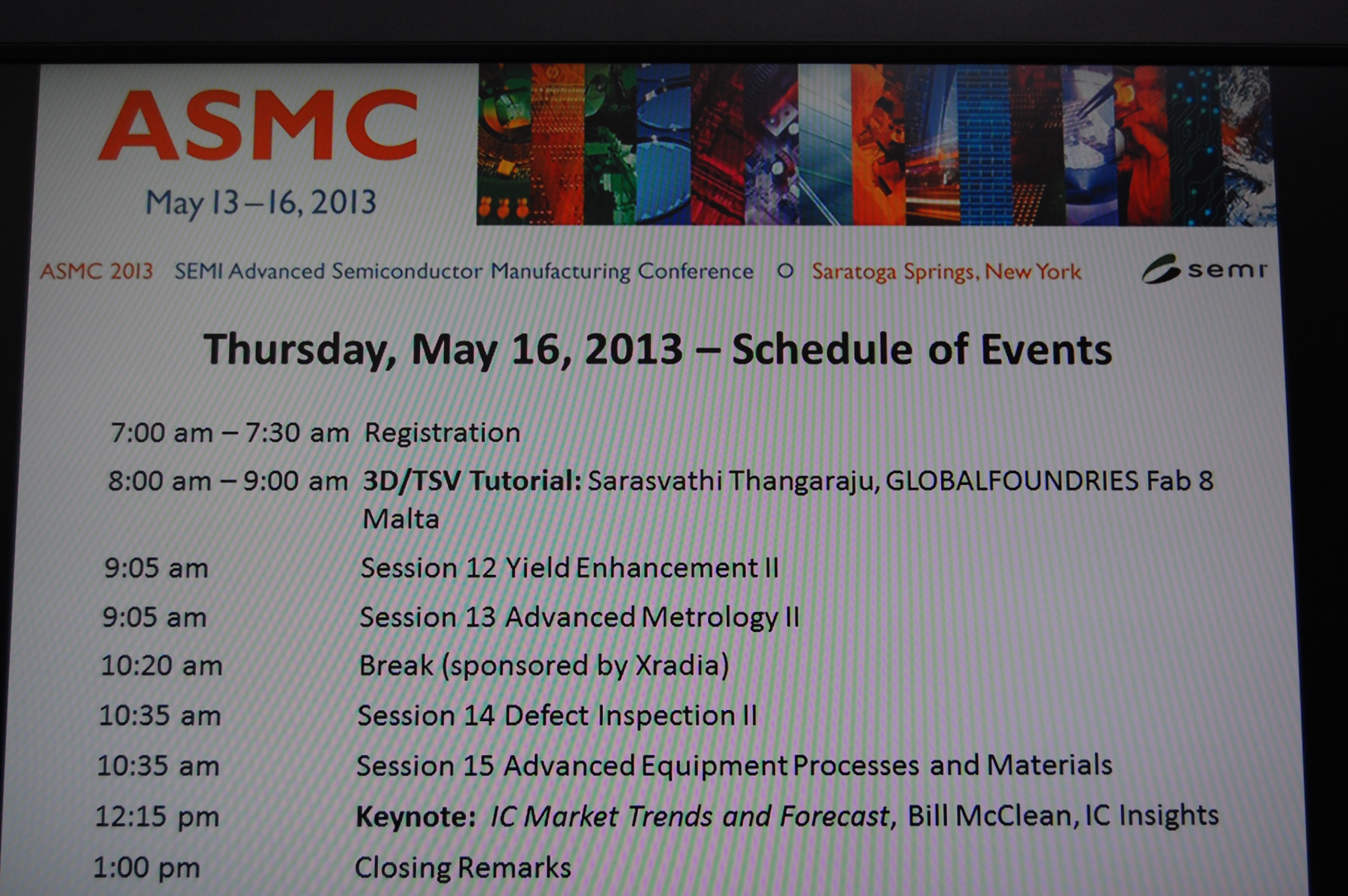
Oh wait – then there’s this bit from Bill McClean, the closing keynote speaker, whose topic was IC Market Trends and Forecast.
Per Bill, with the 20nm planar and the 14nm FinFET process nodes being questionable as to whether they will continue to return the ever-declining cost-per-transistor the industry has generated to date (Moore’s Law), and with the coming transition to 450mm wafers being suspect as well in terms of cost-benefit, it could mean that ASPs for advanced devices will be flat, if not even be rising slightly, over the next few years.
Bill said that state of affairs could be a windfall for new processing technology.
Time to via, for example?
From Petaluma, CA, thanks for reading. ~ PFW


