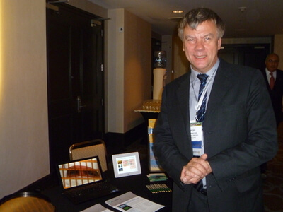
I’ve been on a mission to interview the directors of all three European microelectronics research centers that are participating in the European 3D TSV Summit before the event takes place. So far I’ve checked imec and Leti off the list. Last week, I finally was able to achieve the trifecta when Juergen Wolf of Fraunhofer IZM had time to sit down during the 3D Architectures for Systems Integration and Packaging Symposium (3D ASIP), which took place December 12-14, 2012 in Redwood City, CA.
I was curious about how things have progressed since we last met in March when I visited the Fraunhofer IZM-ASSID facility in Dresden. (If you haven’t already seen it, here’s the video that came out of that visit.) And also how Fraunhofer’s approach differs from its counterparts in Belgium and France; because while all these institutes are essentially competitors, there’s also a lot of collaboration among them for European projects.
In Wolf’s presentation on Friday, his main message was that there can’t really be a general approach taken with 3D integration technologies. Each one is defined by specific requirements of the application. Fraunhofer’s goal is to offer a platform of technologies for applications from which customers select. This is necessary to make it a cost effective solution, explains Wolf. “Customers come to us with a ‘wish list’, but often are speaking at a different level than the technologists,” said Wolf. “Its important for us to understand what they need.” For example, by discussing TSV integration with the IC designer and/or the product developer before he designs a device, he/she can understand what the technical approaches are, and we can find optimal solutions to meet his requests. “It needs to be defined in the beginning before you start anything,” he explained.
Since last March, Wolf says Fraunhofer IZM-ASSID has made “excellent progress” in collaboration with material and equipment suppliers, e.g. ATOTECH, AMAT, EVG and Oerlikon, for the through silicon via filling (TSV) processes, based on test configuration, chemistry analytics and process knowhow. “We can provide a good, stable process for TSV filling,” said Wolf.
Additionally, Wolf reports the very first implementation of a fully functional, active 300mm TSV circuit wafer at ASSID. He stressed that this is NOT an interposer technology. In fact, one key differentiator between Wolf’s approach to developing 3D ICs and others is that he believes its best to fully develop the process for the more challenging technology first (in this case via- mid/last 3D ICs), working with the foundry and the service provider. Once the process is developed, it can be applied to interposer approaches as well. Wolf says it doesn’t make sense to develop the process for the simpler application first, and then need to upscale it to the more complicated application. This top-down approach is very important in order to understand all interfaces and interactions in the complete process.
Fraunhofer IZM developed and demonstrated one of the first passive 2.5 interposer approaches for digital applications several years ago. One of Wolf’s pet projects at Fraunhofer IZM ASSID involves integrating multiple die to create an active interposer. The modular structure allows for stacking on a reconfigurated wafer that serves as an interposer. This all-silicon system-in-package (SiP) is achieved by embedding heterogeneous active dies into a silicon wafer, rather than in mold compound. The wafer acts as a silicon housing, and integrates different functional die into one system. This allows for customers to requisition die from different suppliers and integrate them into one cost efficient wafer level package. This project might be one of the topic of Wolf’s presentation at the European 3D TSV Summit, January 22, 23 2012 in Grenoble.
Wolf says he thinks its good to hold an event like the European 3D TSV Summit to show the opportunities and possibilities, and share what everyone is doing – in particular the research institutes in Europe.
What differentiates Fraunhofer IZM ASSID from IMEC and Leti, says Wolf, is that while the latter two organizations are autonomous unto themselves, Fraunhofer as an organization comprises a number of entities with locations around Germany, and especially in Saxony, each charged with specific development areas. Fraunhofer IZM-ASSID is one arm of the institute, focusing on TSV copper processes for 3D all-silicon system integration based on interposer and TSV via middle/last approaches.
For Fraunhofer, the goal is to “support the industry and not just one customer,” he said, “Our task is to exploit the results.” Fraunhofer IZM-ASSID is interested in promoting 3D integration in different application fields, understanding failure analysis and reliability issues, and ultimately providing application-specific solutions for small, medium and large enterprises worldwide. ~ F.v.T


