
 This year’s European 3D Summit in Dresden, which highlighted “Heterogeneous Integration Driving 3D”, was led off by presentations and a lab tour of the Fraunhofer Institute, whose 18 high-performance centers collaborate with companies, universities and other research institutes in Germany. All pictures and diagrams courtesy of Fraunhofer IZM.
The Fraunhofer IZM presentation was introduced by Jürgen Wolf. Fraunhofer conducts research in microelectromechanical systems (MEMS), spatial light modulators, light detection and ranging (LIDAR) for autonomous automotive applications, embedded non-volatile memory, and medical imaging. They perform research and development (R&D) and pilot fabrication for packaging and MEMS and offer advanced failure analysis and reliability investigation.
X-ray tomography for 3D Heterogeneous System Integration and Product Reliability
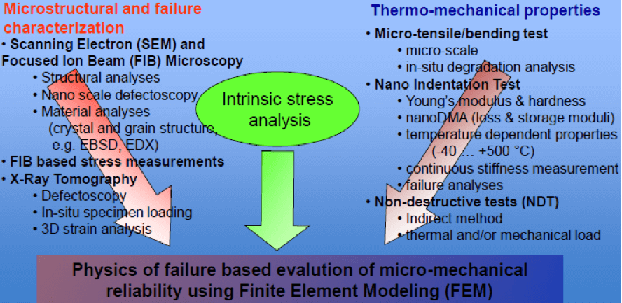
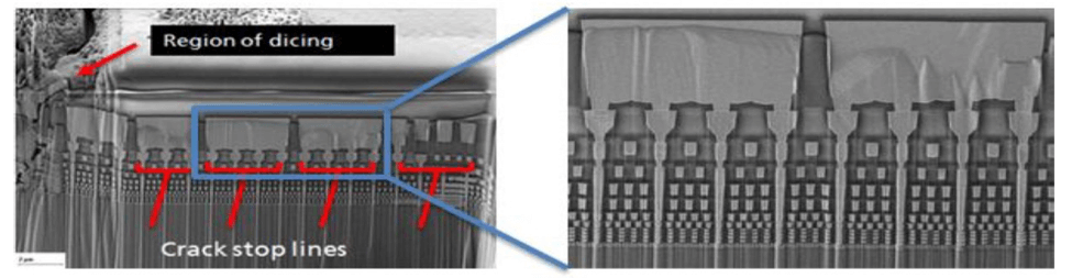
New material combinations with very different coefficients of thermal expansion (CTE) in advanced packaging are causing new reliability challenges. These appear as delamination in weak insulating materials (ultra-low-k) in the back-end of line (BEOL) metal stacks, and cracks in 3D through silicon via (TSV) and redistribution layer (RDL) structures. Additional failures are seen as micro-cracks in thinned silicon and failures in micro bumps. These are related to stress-induced lifetime reduction, electromigration, stress-induced voiding and time-dependent dielectric breakdown.
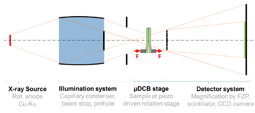
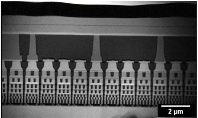
X-ray computed tomography (XCT) is used for analysis of reliability failures. The X-ray source is a rotating anode producing monochromatic radiation based on Cu-Kα (8 keV) radiation (Figure 2)
.
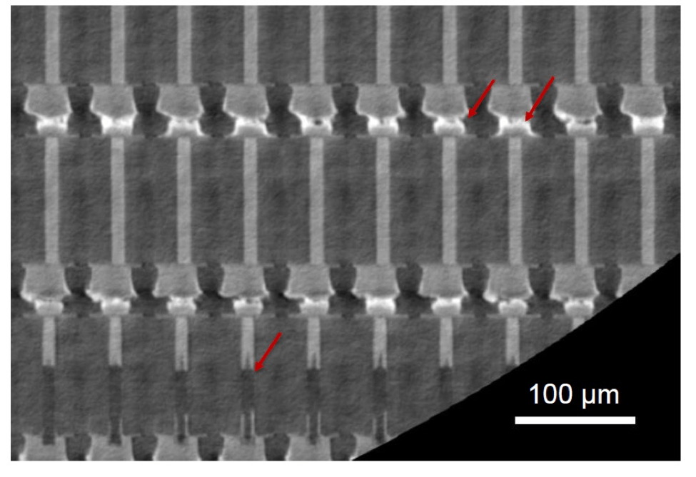
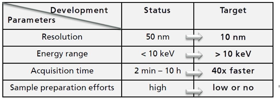
The laboratory is planning the advanced nano XCT for advanced packaging and interconnect imaging for nondestructive 3D analysis with higher resolution and higher throughput.
Fraunhofer High Performance Center
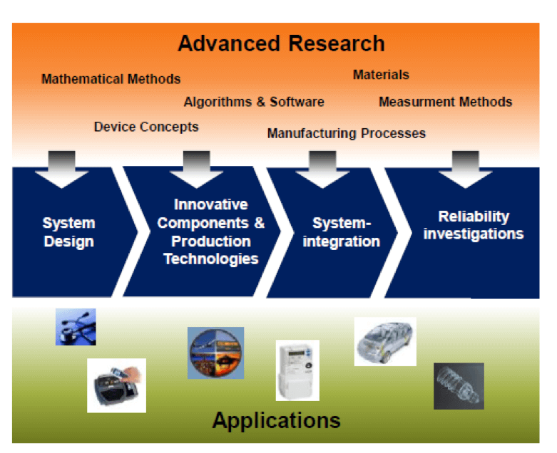
The High Performance Center focuses on innovative components, heterogeneous system integration, and reliability. Innovative electronic system-level design (ESL) leads intelligent IPs, design for reliability and intelligent optical sensors. Library development and models of MEMS sensors are described. Intelligent IP block generators are used for programmable gain amplifiers, ultra-low power ADCs and bandgap voltage references.

A vision system-on-chip has been developed utilizing highly-parallel on-chip image processing. A 2D magnetic field sensor has been developed using GMR (Giant MagnetoResistance)-based spintronics which will allow position and rotation detection for automotive and geolocation applications. A lithium-based 3D thin film accumulator with a solid electrolyte enables energy storage for low power wafer system-in-package (SiP) integration.
Heterogeneous system integration using via-middle and via-last Cu-filled TSVs with a high aspect ratio is being used in interposers and active devices. Interposers are being developed with embedded active and passive devices and advanced active cooling using microfluidics.
Advanced Cu-Cu bonding (DBI Bond®) technology is being jointly developed with Xperi and IZM ASSID. Advanced chemical mechanical polishing (CMP) is used to planarize the wafer surface to <5nm planarity and allows hermetic bonding of the SiO2 at low temperatures (300°C).
Advanced reliability and stress measurement methods enable material and simulation models for the thermo-mechanical reliability of electronic materials. Finite-Element modeling approaches are being applied to 3D-stacked packages.
Fraunhofer continues its leading role in system-level design, design automation, and development of key technologies for advanced packaging.


