
Last week, CEA-Leti launched its Open 3D initiative to the 3D world in an effort to make its mature 3D technologies accessible to industrial and academic partners for their advanced products and research projects. Wanting to learn more about this offer than was detailed in the press release, I interviewed Leti’s David Henry, Open 3D project manager. He not only provided answers to my questions, he also addressed those of M.P. Divakar, a 3D InCites member who posted questions on the press release post itself. (See how this interactive community thing works when people use it?)
Henry explained that rather than addressing the mainstream of 3D, as is the case with TSMCs end-to-end supply chain model, the Open3D offer is targeted towards niche market players. “In our case, the object is to use TSV technology for academic, fabless and niche markets customers,” he said. “We’re offering mature 3D technology to decrease the final cost of the project and also reduce the R&D portion of the project thanks to a shorter cycle time and moderate cost compared with classic R&D projects.” Henry explained that utilizing mature technologies that have already been successfully transferred to industry –– in new projects, gives R&D a head start, versus classical R&D approaches.
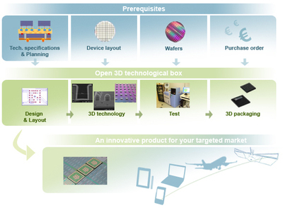
Here’s how it works: interested customers provide Leti with their product’s technical specifications; a “soft version” of the device layout and the necessary device wafers. Before a project is accepted by Leti, it needs to be evaluated to make sure it’s a ‘fit’. “During the specification phase we have a discussion with the customer to analyze their final requirements. If the specifications fall outside of the scope of Open-3D, i.e. the more mature 3D technologies at CEA-Leti, then of course we can offer a more tailored collaboration of larger scope, but not necessarily limited to the ‘plug and play’ technology of Open-3D,” explained Henry. Once cleared for participation, Open 3D provides end-to-end processes including design and layout, 3D technologies, final electrical test, and packaging processed outsourced to a local packaging house.
Open 3D technologies includes via-last TSVs with aspect ratios to 1:3; chip-to wafer microbumping; chip to substrate copper pillar bumps; redistribution layer (RDL); under-bump metallurgy (UBM) and temporary bonding, thinning and debonding; with more to be added as they reach maturity.
As there are still processes with rather large question marks (temporary bonding and debonding particularly comes to mind) I asked Henry to clarify what he meant by “mature technologies.” He said while these technologies may not be considered fully mature from the industry’s point of view for volume manufacturing, they are mature from the perspective of classical R&D. Additionally, some of the technology modules are more mature than others, such as via last TSVs and copper pillars, while some still need further development. As an example, Henry cited work in 2008 to transfer core TSV technology from Leti to ST Microelectronics for use in CMOS image sensors. In 2009, the TSV process matured further due to prototype development, resulting in improved electrical yield.

While TSV is at the high maturity end of the Open 3D offer’s technology catalog, temporary bonding and debonding – particularly debonding – is the least mature of the technologies being offered. “Leti is currently working with a selection of leading equipment and material suppliers in the area of bonding and debonding in order to achieve high-volume manufacturing with the debonding process,” explains Henry, adding that lots of tool and material supplier R&D teams around the world are working to solve this. Citing the different material & tools suppliers that LETI are working with, he says there is beginning to be industrial tools for this, which is an improvement on the past 2-3 years, when only lab tools were available. Henry says he’s optimistic to have a solution before the beginning of next year.
“In Open 3D, the maturity of the technology bricks is not the same for all the bricks, but overall, the R&D effort for the customer is clearly lower than in classical R&D project,” he explained, “Since there is no need to spend R&D effort on TSV and copper pillar, we can focus the effort on temporary bond and debond, and still have an overall shorter cycle time and lower cost.”
Citing TSMC’s model as a comparison point, M.P. Divakar inquired whether Leti has a model for transferring this concept to high volume manufacturing. Henry’s response – it’s in the works. For the moment though, he says the Open 3D offer extends from proof-of-concept through prototyping and low volume production. “If we have a customer who needs to go to HVM, we are in discussions with a partner who would handle the technology transfer from low to high volume,” said Henry. Ultimately, the model calls for one HVM partner, and discussions are in progress with a third party. “If we work with the same partner, the technology transfer has been done before and it’s easy to pass it off each time.” However, that’s not to say Leti won’t offer the flexibility of working with a customer’s preferred foundry if required. And therein lays another difference with TSMC’s end-to-end model. Will TSMC be as willing to work with chips from different sources and apply 3D technologies to those? Henry says there are customers who require the flexibility of a foundry willing to work with a smaller number of wafers as well as different chip sources. Open 3D provides that option. ~ F.v.T.


