


Staying relevant in the ever-expanding technology landscape that is the semiconductor packaging industry can be a struggle for an event that’s been laser-focused on one emerging segment since its inception. But this past week, 3D Architectures for Semiconductor Integration and Packaging (3D ASIP 2015) delivered a program that not only addressed the progress of 3D integration, it also expanded the conversation to include other developments in high-density advanced packaging (HDAP), and heterogeneous system integration.
While previous editions of this event focused primarily on processes and technologies for through silicon via (TSV) fabrication and subsequent backside processing steps for interposer and 3DIC devices, as the technology reaches maturation, attention has shifted to what products are implementing 3D, and how do we address power, performance, area, and cost (PPAC) for consumer electronics applications. Essentially,
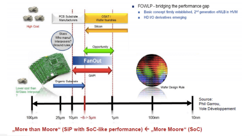
As Thibault Buisson, Yole Developpement explained during his plenary talk, Comparison of New Memory Architectures, continued scaling is widening the disparity between printed circuit board (PCB) feature sizes, and CMOS feature sizes. 3D TSV and fan-out wafer level packaging (FOWLP) are filling this gap (FIgure 1). As predicted for years, the memory market is emerging as the next bastion of TSV growth and adoption. Indeed, 2015 will go down as the year of 3D TSV stacked memory.
According to Buisson, graphics cards have been first application to use 3D stacked memory. Additionally, he says many leading OEMS plan to release new products using HBM and hybrid memory cube (HMC) memories targeting HPC applications like networks, routers, and switches. Additionally, Toshiba has implemented TSVs in its 3D NAND. Furthermore, new products will be Si-interposer based, or directly integrated on the PCB, and could contain multiple ASICs and multiple memory cubes.
Presentations by Minsuk Suh, SK Hynix; Kazuyuki Higashi, Toshiba; Tom Gregorich, Micron; and Bob Patti, Tezzaron Semiconductor, further drove home the availability of a plethora of 3D DRAM technologies implementing TSVs, and the reasons why.
Suh noted that HBM has overcome all the DRAM challenges for high bandwidth memory. While TSVs are still an expensive technology, he says they are already in mass production in high-end applications, which will help decrease the cost.
One of the year’s biggest success stories that implemented HBM and interposer technology is AMD’s Radeon Fury, which has been making headlines as the first implementation of 3D High Bandwidth Memory (HBM) integrated into the Fiji GPU. Bryan Black presented a talk, The Road to The Fiji GPU”, offering an inside look at all that was involved to get there. “Now that we’ve done the Fiji Chip – we’ve figured out how to do this, and we can do it in anything,” he said.
Calling TSVs ‘the most promising technology for future” Toshiba’s Higashi noted that in comparison to wire bond, TSVs offer 10X the inter-chip connections at <1/10th parasitic capacitance to achieve high speed and low power. Moreover, Toshiba has adopted a backside via process for its TSV NAND because they believe it to be a lower cost approach than via-mid, because it requires fewer process steps.

Gregorich noted that while there’s consensus that the 3Di TSV DRAM cube is a good idea and is demonstrating good yields in different high performance computing applications, the solution for consumer products may be different because each segment (PC, tablet, phone, wearable) has unique requirements (ie: density, bandwidth, form factor, power usage, power handling, low cost). “While solutions for the consumer markets might be based on 3D TSV DRAM cubes, the interface between the DRAM and the CPU is the key to providing low-cost, high bandwidth, and low power,” he said. “The challenge is how to adapt it into other markets.” The smartphone, for example, is very dependent on package-on-package (PoP) structure. How do we adapt the PoP to wide interface so we can continue with that structure but still put TSVs in it.
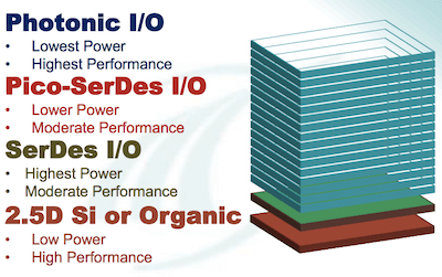
According to Patti, we will see revolutionary changes over the entire market in the next 3-5 years, and the future is definitely about More than Moore. “How do we put all these things together? We’ll have a super computer the size of a softball,” he said. At Tezzaron, the focus is not only on storage-class memory, but on integration of different functional layers that Patti breaks down into memory bit layer, controller layer, and I/O layer. The I/O layer could be Pico-SerDes, SerDes, or photonics; whichever is needed (Figure 2). This is stacked on a Si or organic interposer, based on density requirments. Tezzaron has the foundry platform to support all of this.
Let’s remember that 3D TSVs are only one option in the HDAP wheelhouse. While we are told cost will come down naturally as 3D TSV volumes in high performance computing applications take hold, research and development on other high-density approaches didn’t come to a screeching halt while we were trying to solve issues with TSVs. Ultimately, it’s not an “us vs. them” conversation. It’s a “which technology is the best suited to the job at hand” conversation. Brandon Prior, Prismark Partners, pointed out that adoption of 3D integration doesn’t just require process technology to be there, but also requires alignment of image sensor, logic, and memory die size to be cost effective.
Prior also noted that Intel and Samsung remain skeptical of FO-WLP. At this time, neither have plans to install fan out capacity, and it’s not seen as cost-effective means to make a thinner package. However, the expectation that Apple will proceed with TSMC’s integrated fan-out (InFO FO-WLP) for the A10 processor in 2016 is enough to make other major industry players like SPIL/Xilinx, Amkor, Deca, and many others step up their offerings in the HDAP space.
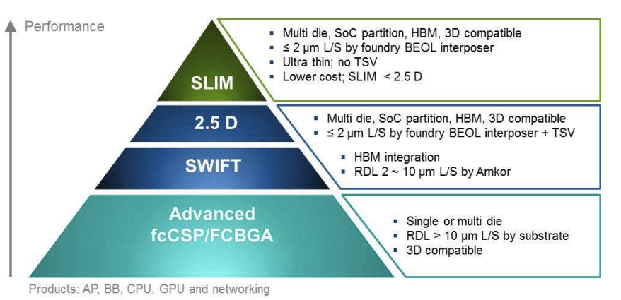
One thing was made clear through three days of presentations — varied options are not in short supply. In addition to TSMC’s KC Yee, who espoused the benefits of TSMC’s InFO technology, we also heard from Dyi-Chung Hu, of Unimicron, who introduced embedded high-density film (eHDF), a high-density substrate platform that eliminates the need for TSVs (he called them TXVs), Si interposers, and underfill. And we heard from Xilinx Fellow, Suresh Ramalingam, who talked about the company’s silicon-less interconnect technology (SLIT), which also eliminates the need for TSVs. Lastly, Amkor’s Mike Kelly talked about the company’s many options to address line/space requirements at different sizes to address the gap between 1µm and 8µm l/s from it’s most advanced technology, silicon-less interposer module (SLIM) that doesn’t use TSVs; to the now conventional 2.5D/3D solutions to silicon wafer integrated fan-out (SWIFT), to address 2-10µm l/S.
Differentiating between all these HDAP offerings that are suddenly available is a daunting task. But as Yee noted in his presentation, the more options available to the customer, the better. Perhaps it’s time to lose the 3D and rename this conference, High-Density Architectures for System In Packaging? Ah yes – and we didn’t even touch on the heterogeneous integration portion of the event. Yet. More to come! ~ FvT.


