PLANOPTIK AG News
The Growing Importance of Glass Substrates in Semiconductor Technology
The semiconductor industry is experiencing a significant shift towards the use of glass substrates, driven by their superior performance characteristics...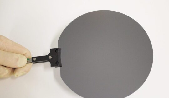
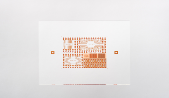
Discover Wafer Universe: Your Premier Source for Standardized Wafers
Plan Optik AG is excited to introduce Wafer Universe, crafted to meet the urgent needs for standardized wafers with a...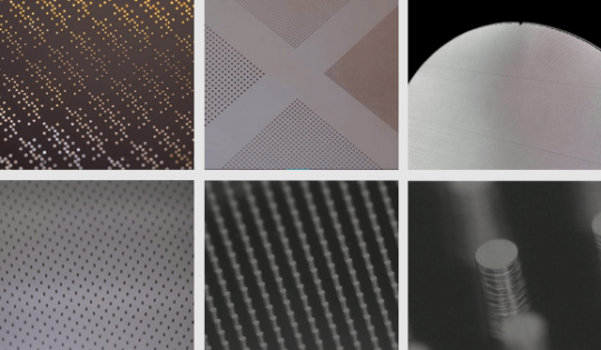
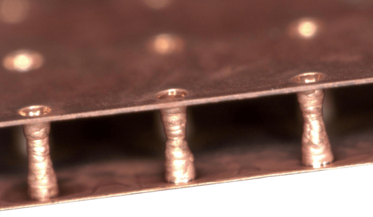
Plan Optik and 4JET Jointly Develop New Process for Advanced Packaging
• Process innovation for through-glass vias in the field of advanced packaging • Premiere at Touch Taiwan on April 19-21...
Plan Optik Develops New Advanced Connectivity Technology (ACT) for 3D-Integration, 5G and Other Connectivity/High Frequency Applications
Plan Optik is the leading manufacturer of customized glass wafers. In sectors such as consumer electronics, automotive, aerospace, chemistry and...
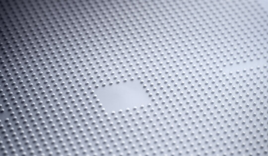
Glass Carrier for GaAs Wafer Processing
Gallium arsenide (GaAs) is used in the manufacture of devices such as microwave frequency integrated circuits, monolithic microwave integrated circuits,...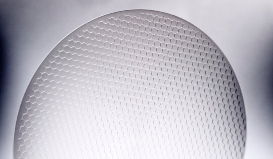
Carrier Wafers for Semiconductor and MEMS Manufacturing
As technology rapidly moves forward, the reduction of device and chip size is playing an important role in implementing as...