At the recent ECTC conference in Dallas, IBM and DECA announced the signing of an agreement to implement Deca’s M-Series...
The U.S. Investment Accelerator was officially established on March 31, 2025, as part of an effort to modernize the investment...
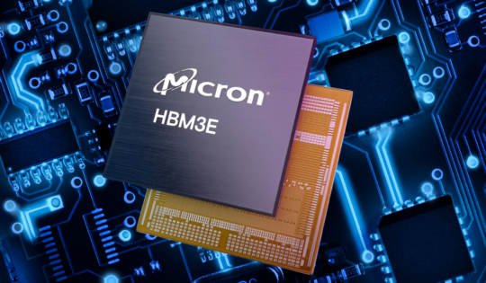
HBM is one of the hottest markets right now thanks to the tremendous demand for AI GPU computing power. HBM...
Earlier this year GlobalFoundries (GF) announced a New York Advanced Packaging and Photonics Center (NY APPC) billed as “…the first...
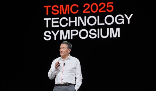
Dr. Cliff Hou, Senior Vice President and Deputy Co-COO (above), spoke at this year’s 2025 Technology Symposium. highlighting TSMC’s continued...
In IFTLE 626 we looked at the Yole article that addressed the question of whether panel level processing was finally...
Is TSMC Acquiring 20% of Intel fabs? Reports are that Intel and TSMC have reached a preliminary agreement to form...
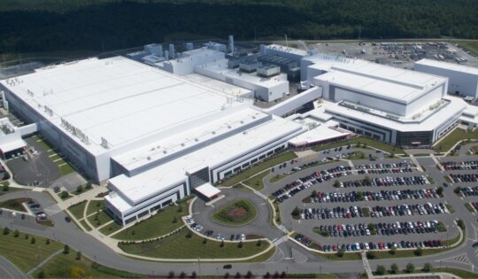
An aerial view from February 2024 shows construction progress at Intel’s Ohio One campus of nearly 1,000 acres in Licking...
TSMC widens edge over Samsung The Taipai Times recently offered the following interesting discussion concerning the TSMC versus Samsung rivalry:...
TSMC Invests Further in Arizona Taiwan Semiconductor Manufacturing Corporation (TSMC) plans to make a $100B investment in the United States...
When I was first asked why I had not yet covered the “US Joint Consortium” I responded “tongue in cheek”...
Commercial Times reports that TSMC’s Arizona wafer fab, Fab 21 Phase 1, has officially entered mass production on its 4nm...
Micross, a portfolio company of Behrman Capital, announced on January 15, that it has acquired Integra Technologies, headquartered in Wichita,...
CHIPS for America has announced three anticipated CHIPS for America research and development (R&D) flagship facilities. These state-of-the-art CHIP flagship...
Multi-die systems are driving the need for standardized die-to-die interconnects. Several industry alliances have come together to define such standards:...
Will TSMC, SK Hynix, and Amkor be an Onshore Source for Nvidia? SK Hynix learned to package its own stacked...
Broadcom has recently announced the availability of its 3.5D eXtreme Dimension System in Package (XDSiP™) platform technology, enabling consumer AI...
TSMC recently announced at its Open Innovation Platform (OIP) Ecosystem Forum in Europe that its chip-0n-wafer-on=substrate (CoWoS) packaging technology will...
Intel Reaches The Fork in the Road Digitimes had some interesting recent opinions about the future of Intel. Let’s take...
We have seen considerable global activity focused on developing glass core substrate assemblies and interposers, yet, as some of us...