
HBM is one of the hottest markets right now thanks to the tremendous demand for AI GPU computing power. HBM manufacturers SK Hynix, Samsung, and Micron are all competing for control of the market. As it stands now, most feel that Hynix is in the lead.
As IFTLE has reported, SK Hynix plans to build a new advanced memory packaging facility in Indiana, starting operations in the second half of 2028. This facility will focus on HBM4 and HBM4E memory products. The facility will not process wafers with memory circuits but will assemble HBM from known good stacked dies consisting of multiple memory dies on top of a base die.
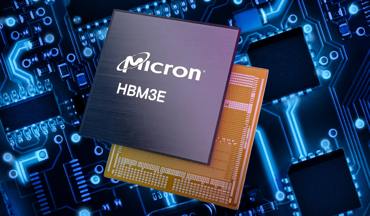
Micron Technology has received $6.1B from the CHIPS Act to expand its manufacturing in Idaho and NY. The company has reported that it plans to secure 20-25% of the HBM3E market share by August 2025.
Micron also reported that its HBM production was sold out in 2024 and 2025. The company claims that the progress in its HBM3E is due to its advanced packaging and design capabilities, as well as the integration of its own processes.
Micron is also working on next-generation HBM4 memory. HBM4 memory, with a 2048-bit interface, is planned for mass production in 2026, with HBM4E to follow. In addition to offering higher data transfer rates than HBM4, HBM4E will also introduce an option to customize its base die. The custom logic dies are set to be made by TSMC.
It is unclear whether an actual JEDEC standard supports such customizations. Micron says that its development work on HBM4E products is well underway with multiple customers, and that we should expect different customers to adopt base dies with different configurations. They hope this results in “…customized memory solutions for bandwidth-hungry AI, HPC, networking, and other applications.”
Micron’s HBM4 will use the company’s DRAMs made on its 5th Generation 10nm-class process technology, placed on top of a base die featuring a 2048-bit wide interface and a data transfer rate of around 6.4 GT/s, which will provide a peak theoretical bandwidth of 1.64 TB/s per stack. Micron plans to ramp HBM4 production in high volume in calendar year 2026, which aligns with the launch of Nvidia’s Vera Rubin and AMD’s Instinct MI400-series GPUs for AI and HPC applications.
GaN for RF
In the May 7th issue of EE Times, Emily Newton wrote an article entitled “Why RF Technologies Should Consider GaN Over Silicon”. [link] It’s worthwhile reviewing what she has to say.
While she admits that the use of GaN technology in RF applications is still relatively niche, she contends that it will increase significantly due to the impressive GaN benefits that have been uncovered including:
Power Density
The biggest advantage of GaN for RF components is reportedly its power density. It’s bandgap (3.4 eV) when compared to silicon ( 1.1 eV) means it can higher power and faster switching without performance degradation.
That is especially important to 5G. 5G’s higher frequencies and broader range of frequency bands require additional power to maintain communications with no signal loss.
GaN also reportedly “ lasts longer than silicon in high-frequency RF use cases”. Newton claims that military, aerospace and industrial IoT devices would benefit he most from such longevity.
Thermal Performance
GaN semiconductors show better thermal performance than silicon alternatives, especially during high loads which can be critical for RF technology. Better thermals also enable smaller device form factors, as there is less need for external cooling systems.

Efficiency
GaN’s wider bandgap enables power conversion with fewer losses than conventional silicon solutions, which allows for lower power RF components. GaN’s conversion efficiency also results in a better signal This is particularly valuable for 5G networks, which already deal with shorter ranges but higher frequencies than previous mobile technologies.
Size Benefits
GaN circuits can support the same energy and frequency with less material, thus the entire PCB can shrink. Compact PCBs can also be beneficial for thermal management, as there is more room in the end product for cooling fans and similar components..
Remaining Obstacles to GaN RF Technologies
Despite these considerable benefits, GaN technology still has issues.. GaN is costly. A two-inch GaN substrate can cost as much as $1,900, compared to just $50 for a silicon alternative. Combining GaN and silicon carbide (SiC) is reportedly more cost-effective, but these solutions are still 50% more expensive than an entirely SiC option according to Newton.
GaN supply is reportedly also an issue.. “… 98% of primary gallium currently comes from China and China has banned the export of gallium and germanium to the U.S., leaving American RF companies with few options for sourcing the materials necessary for GaN semiconductors”. Gallium is a by-product of aluminum production, so RF companies may be able to bolster their gallium supply chains by partnering with aluminum manufacturers outside of China. Re-shoring gallium production by partnering with domestic aluminum foundries will hopefully ease cost and supply concerns.
While it is accepted that it will take time before GaN technology scales up to where it needs to compete for widespread implementation in RF applications Newton expects the telecom industry especially will continue to move ahead because of its potential.
For all the latest in Advanced Packaging stay linked to IFTLE……………..


