
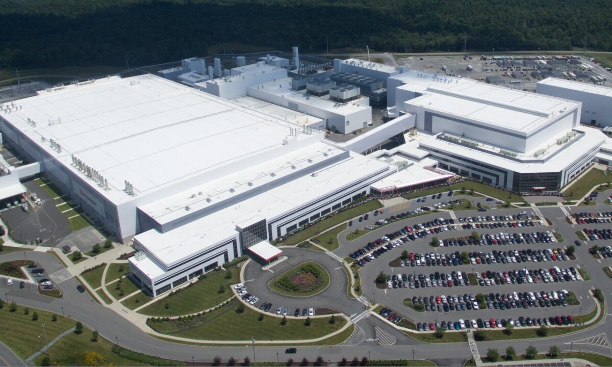
Earlier this year GlobalFoundries (GF) announced a New York Advanced Packaging and Photonics Center (NY APPC) billed as “…the first of-its-kind center to offer advanced packaging and test capabilities in New York for U.S.-made essential chips used in AI, automotive, aerospace and defense, and other applications” at their Fab 8 site in Malta NY (Above image: GF Fab 8 Malta, courtesy of GlobalFoundries)
They noted that advanced packaging has emerged as a critical enabler for highly differentiated microelectronic solutions. “The capabilities in this center extend beyond GF’s wafer manufacturing to enable securely manufactured, processed, packaged, and tested products for our customers entirely onshore in the United States.”
GF’s NY APPC will reportedly offer:
- Advanced packaging, assembly and testing for GF’s differentiated silicon photonics platform, which brings together optical and electrical components on a single chip to realize power efficiencies and performance advantages.
- Full turnkey advanced packaging, bump, assembly and testing for aerospace and defense customers under GF’s Trusted Foundry accreditation, allowing chips used in sensitive national security systems to never leave the U.S. during production.
- New production capabilities for the advanced packaging, wafer-to-wafer bonding, assembly and testing of 3D and HI chips using GF’s 12LP+, 22FDX®, and other leading platforms.
Volume ramp is expected in 1st half of 2028.
GF’s overall investment is expected to be $575 million, with an additional $186 million investment in research and development over the next 10-plus years. New York state will provide up to $20 million in new support for the new center, which is in addition to the previously announced $550 million in support for GF from the New York State Green CHIPS program. The U.S. Department of Commerce will provide up to $75 million in direct funding to support the center, supplementing the previously announced GF award under the CHIPS and Science Act.
IFTLE contacted GF to get a little more detail on what they were planning. They laid out the following description for their GF end-to-end Advanced Packaging and Photonics Services and showed the following description of their proposed products and processes.
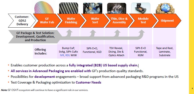
They report they will be using first-of-a-kind test solutions developed with industry partners to offer complete electro-optical test coverage across wafer, chiplet, and fully packaged parts that delivers ultra high-speed capabilities.
They also report that there will be no change to their current assembly and test services. They will continue to use their current OSAT partners.

New Government Office set up to manage CHIPS Act
The new administration has set a new entity to take over the CHIPS Act program and speed up corporate investments in the United States.
The United States Investment Accelerator within the Commerce Department will oversee implementing the CHIPS and Science Act. The new office will be responsible for “negotiating much better CHIPS Act deals than the previous administration,” the White House said, without providing further details on what would be negotiated.
The Investment Accelerator will also encourage companies to make large investments in the U.S. by reducing regulatory burdens, speeding up permitting, coordinating with federal agencies and states, and increasing access to national resources, according to a fact sheet released by the White House.
For all the latest in Advanced Packaging stay linked to IFTLE…………………………..


