
![]() The U.S. Investment Accelerator was officially established on March 31, 2025, as part of an effort to modernize the investment landscape in the U.S.
The U.S. Investment Accelerator was officially established on March 31, 2025, as part of an effort to modernize the investment landscape in the U.S.
According to the announcement, the “Investment Accelerator” will be headed by an Executive Director and staffed with legal, transactional, operational, and support staff as directed by the Secretary of Commerce.
Its primary goals include:
- Assisting investors as they navigate regulatory processes
- Reducing regulatory burdens, and identifying any existing mechanisms, exceptions, and opportunities in Federal law that can be used to assist foreign and domestic investors, consistent with the protection of national security
- Increasing access to and use of national resources
- Facilitating research collaborations with national labs
- Working with State governments in all 50 States to reduce regulatory barriers to, and increase, domestic and foreign investment in the United States.
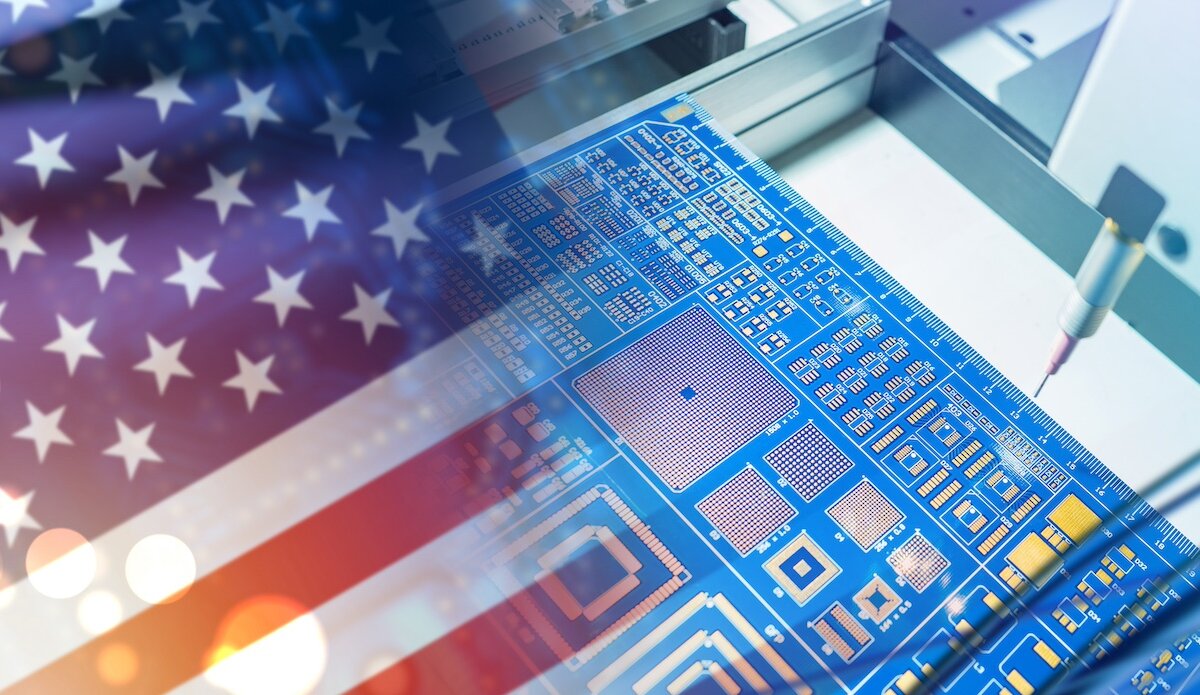
- Administration of the CHIPS Program
The United States Investment Accelerator within the Commerce Department will oversee implementing the CHIPS and Science Act, the 2022 law that made $52.7B available for semiconductor chips manufacturing and production.
This new administration indicated that the Investment Accelerator will be responsible for “negotiating much better CHIPS Act deals than the previous administration,” without providing further details on what would be negotiated.
According to Bloomberg, Commerce Secretary Lutnick is negotiating with investors to increase the size of their investments without increasing the awarded funding provided under the CHIPS Act. Subsequently, TSMC, said it would add $100 billion to its initial $65 billion investment plan in a fab complex in Arizona. There have been no other public responses from manufacturers involved in new fab projects.
The Commerce Department has reported that more than 50 fabs, fab expansions, and R&D sites are currently underway in 28 states under CHIPS Act funding.

At the site, “Tracking CHIPS and Science Act Awards”, one can find the complete listing of current award winners. Let’s take a look at some of these winners, including quite a few that we have not discussed previously on IFTLE.
- TSMC: $6.6B for activity in AZ which includes at least five advanced fabs and packaging The first fab is already operational.
- Intel: $7.9B towards building two new fabs in Ohio and expanding facilities in Oregon, New Mexico and Arizona.
- Samsung: $4.7B for a new fab in Taylor, Texas for memory and logic.
- Micron: $6.2B towards two NY facilities and one Idaho facility. Micron is expected to onshore approximately 40% of their DRAM chip production over the next 20 years. Also awarded $275MM to expand and modernize its Manassas, Virginia, facility.
- Texas Instruments: $1.6B toward a new fab in Lehi, Utah and expansion in Sherman TX.
- GlobalFoundries: $1.5B for expansion of its New York fabrication facility to triple wafer capacity production, as well as update its Vermont site.
- Wolfspeed: $750MM for a new SiC wafer manufacturing facility in NC and expansion of a device manufacturing facility in New York.
- Amkor: $407MM for Advanced Package and assembly facility in AZ.
- SK Hynix: $458MM for artificial intelligence products and an advanced packaging fabrication and R&D facility.
- Microchip Technology: $162MM for factory expansion projects to increase domestic production of microcontrollers and other related semiconductor products.
- BAE Systems: $35MM to quadruple production of its advanced chips for military and satellite applications.
- Analog Devices: $105MM for investment in its Massachusetts manufacturing sites to boost module production for commercial, space and defense applications. CHIPS funding for its Oregon and Washington sites would expand mature node semiconductor manufacturing by 70%, onshoring key process nodes like 180 and 350nm.
- Corning: $32MM to increase production of high-purity fused silica
- Edwards Vacuum: $18MM to make dry vacuum pumps. There is no domestic production of semiconductor-grade dry vacuum pumps, according to the Commerce Department.
- Infinera: $93MM to help build a semiconductor fab in San Jose, California, and an advanced test and packaging facility in Bethlehem, Pennsylvania.
- Coherent: $33MM to support expansion in Texas of 150mm InP manufacturing line and $79MM for the fabrication of 150mm and 200mm silicon carbide substrates in Easton, Pennsylvania.
- Sumika Semiconductor Materials: $52MM for the manufacture of high-purity chemicals in the U.S.
- + several others
Will any other companies up the ante and commit more of their own monies the way the TSMC has? I guess only time will tell!
For all the latest in Advanced Packaging stay linked to IFTLE……………………………………..


