


SEMICON West 2014 brought its usual flurry of supplier announcements on new equipment and process improvements; but there weren’t as many focused on 3D technologies as there have been in past years. This is likely due to the fact that some players are holding off until 3D hits it big and they get some return on their investment. But for the true die-hards, they’re not letting a little thing like delayed adoption stop them. 3D InCites made the rounds to get the details, both on the progress and the delays. Here are some of the highlights we thought were important to share with our readers.
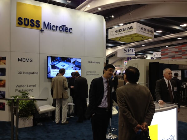 SUSS Microtec introduced its ELD 300, a stand-alone dedicated excimer laser debonder designed to address the ongoing debond challenge that is thought to be one of the reasons 3D ICs have not reached high volume manufacturing (HVM). According to Stefan Lutter, General Manager, Bonder Division, SUSS Microtec, the ELD 300 addresses two issues with current debonding processes: yield and throughput.
Excimer laser debonding is considerably faster than mechanical debonding, explained Lutter. Also, it delivers higher power than traditional lasers used for thermal release processes. It breaks the chemical bonds without generating any heat using cold ablasion. Lutter said SUSS has used excimer laser processes for several years for multiple high resolution patterning in its excimer laser patterning tools, and that excimer laser debonding is quite mature.
The main technical benefit of the ELD is the elimination of lift-off force; the mechanical stress on the device wafer is zero, noted Lutter. ELD only works with glass carriers, but Lutter says that many of the OSATS are open to the idea of using glass carriers vs. silicon carriers.
The reason for introducing a dedicated debonder for HVM is to address the throughput issue. Lutter explained that in an R&D setting, customers prefer that debond and clean modules are in one tool. In volume manufacturing, it makes sense to separate the processes in two steps. A typical cleaning tool with multiple clean modules has a 20/wph throughput and the ELD300 has a 40/wph throughput, so it requires two cleaning tools per debonder to keep up. “In high volume, we need to squeeze every penny out, which is why we’ve come up with a dedicated debonder,” said Lutter. “In a combined tool, the slowest module defines what the overall system throughput is, which lowers cost of ownership (CoO).” According to the company press release on the ELD 300, the tool can also be used as an integrated process module in SUSS MicroTec’s XBC300 Gen2 platform. Lutter says the tool is now in qualification with a leading OSAT customer.
Progress is also being made on the permanent wafer bonding front, with EV Group’s introduction of its Gemini FB XT – the FB stands for fusion bonding. The system features EVG’s new SmartView®NT2, which has demonstrated face-to-face alignment accuracy within 200nm (3σ), exceeding the requirements of the latest edition of the Industry Technology Roadmap for Semiconductors (ITRS). Integrated metrology has also been added into the tool, which validates alignment after pre-bonding to enable customers to quickly fine-tune the bonding process for HVM processing if necessary. Also appealing to HVM is the tool’s 50% increase in throughput due to the ability to accommodate up to six pre-processing modules, faster handling, and improved process flows.
According to Dave Kirsch, general manager, EV Group North America, the tool was developed to support hybrid bonding processes like Ziptronix DBI, and oxide bonding for TSV last integration with very small diameter vias; both require super-high alignment accuracy. EVG is always eager to invest in R&D to enable next-generation devices. In this case it’s 3D stacked memory like high bandwidth memory (HBM), next-generation stacked CMOS image sensors, and 3D monolithic devices architecture.
According to Paul Lindner, executive technology director, EVG, two years ago the company optimized the tool’s distortion (non-linear errors within a scanner field). In developing the next-generation SmartViewNT2 aligner, they focused on further improvement of linear error components (x, y, rotation and scaling). Small non-linear tolerance is important for image sensors, he said.
The high accuracy alignment improvements also enable wafer-to-wafer stacking for HBM where wafers are stacked first then thinned, thereby eliminating the need for temporary bond/debond steps. Kirsch said it’s a very front-end oriented approach that supports via mid or via last. In via last, wafers are stacked, thinned, then etched; Or, vias and interconnects can be implemented after each layer. This process can push to thinner stacks with 1-1µm vias.
In her presentation at the SEMI Press Conference, An Steegan, imec, noted that “hybrid bonding is a key enabler of 3D SoC.” Lindner agrees, citing development activity at both imec and Leti. TSV last has long been the approach for CMOS image sensor technology, and with backside illumination image sensors (BSI) now going into HVM, smaller diameter TSVs are key to bringing down the cost because they reduce the amount of wafer real estate that is consumed. As such, development of this system was “very customer driven,” said Lindner. “Major IDMs and foundries working on existing systems pushed for tighter alignment specs.” Looks like EVG listened to the customers.
 Another company looking ahead to smaller diameter TSVs is SPTS, who recently announced a two-year agreement with Leti under the framework of the Nanoelec Research Technology Institute (RTI). To scale future 3D devices, new techniques will be needed to manufacture TSVs of smaller diameter and higher aspect ratio than are used today.

David Butler, VP marketing, SPTS explained that the agreement is really an extension of a collaboration SPTS already had with Leti. SPTS etch, chemical vapor deposition (CVD) and physical vapor deposition (PVD) equipment has been installed at Leti for some time, and it was used to achieve high aspect ratio (HAR) TSVs of 10:1. Next on the agenda is to achieve the ITRS Roadmap’s goal of 15:1 aspect ratio by 2018.
“PVD gets expensive, and makes the processes that come after it more difficult,” Butler explained. “We need an alternative to PVD, so we’re working with Leti on a solution that implements metal organic CVD (MOCVD).” This process involves depositing a titanium nitride film barrier layer in the TSVs. The process provides more conformal step coverage where the vias stay open, rather than closing over like PVD would for such HAR vias. The second phase of the project will focus on development of a CVD copper seed layer layer, followed by ECD fill.
Target applications for such HAR TSVs includes high performance computing, high bandwidth memory and video chips, said Butler. Is this work critical to adoption of 3D TSVs? Not according to Butler. “The industry will go into production with what they have. After that, they’ll move on to addressing the long-term roadmap.”
By now you’re wondering, what’s with the frog (top of page)? It was part of Nordson DAGE’s booth display, representing the company’s efforts to “measure the invisible.” i this case, voids in bumps and TSVs. David Bernard, of Nordson DAGE updated me on the progress of the XM8000 Wafer X-Ray Metrology tool since I paid the company a visit in January. He had some good news to report. The company has completed construction of its cleanroom manufacturing facility in Alesbury for the manufacturing of the XM8000.
Bernard also reported that the tool’s high speed throughput for inspecting wafer bumps is generating lots of interest. Inspecting an 8” wafer with 1M bumps takes 20 minutes on the XM8000, vs. 8 hours with the old system, he said. According to Bernard, up until now, what people have been doing is inspecting 200 bumps out of a million, which is statistically not satisfactory.
With regard to TSV inspection, adoption hasn’t happened quite as fast, and there is still data being gathered for detecting TSV voids. To compensation for possible image distortion and overlap, an oblique angle view is needed for detecting voids in TSVs, explained Bernard. It may be a matter of going to computer tomography (CT), which takes a bit longer – 10-20 seconds to generate a 3D model – but the improvement in the results may be worth it.
I also stopped by Nordon MARCH to get an update on the company’s progress with the plasma cleaning processes for TSVs, and for surface preparation for bumping that we talked about for the first time at SEMICON West 2013. Plasma descum is used before electroplating to clean the surface of the wafer after wet processes. Plasma is also effective in removing photoresist, and for pre-treatment for Cu pillar – Cu pillar thermocompression bonding. The goal, says Doan, is to remove the Cu oxide layer and then passivate the copper to prevent the oxide layer from growing back for up to 7 days vs. 3 hours without passivation.
The good new is, the company has been so busy filling customer orders for its existing tools that it has temporarily converted its R&D facility to manufacturing. Doan says since we spoke last year, there’s been lots of work with a European consortium to collect data. The tool being qualified is a lab-based tool, rather than a fully automated machine. Introduction of an automated plasma system has been pushed out to Q4, where it will be installed at 2 customer beta sites. ~ F.v.T.


