


Major Foundry Investments in the US
Samsung, Intel, and TSMC are all making large foundry investments in the US.
First reported in May, Samsung Electronics is reportedly now close to finalizing the site selection for its new $17B foundry in the United States. The investment would create a second foundry, the first being in Austin TX.
Business Korea reports that Samsung is negotiating with five city governments in three states: Austin and Taylor TX, Goodyear and Queen Creek AZ, and Western New York Science and Technology Advanced Manufacturing Park. Samsung’s decision appears to be imminent.
In March, Intel announced its re-entry into the foundry business, and a plan to build two semiconductor plants in Arizona and expand existing factories in New Mexico. In July rumors started that Intel was considering acquiring GlobalFoundries, (see IFTLE 492).
TSMC has announced a plan to build a $12B foundry in AZ. (See IFTLE 490 “TSMC Considers Packaging Facility in the US.)
TSMC is the current leader in the foundry market with a >50% share in Q2 2021, followed by Samsung Electronics with ~17%, UMC ~7% percent, and GF and SMIC.
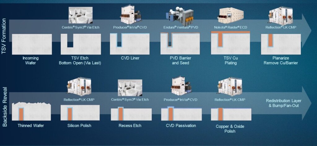
AMAT Holds Packaging Master Class
In early September, Applied Materials (AMAT) introduced several new technologies and capabilities they claimed would accelerate the semiconductor industry’s Heterogeneous Integration Roadmap (HIR). Specifically, they talked about:
- Die-to wafer (D2W) and Wafer-to-Wafer (W2W) hybrid bonding and advanced substrates
- New advanced software modeling and simulation for D2W hybrid bonding at Applied’s Advanced Packaging Development Center to speed customer time-to-market
- Entering into a joint development agreement with EV Group for co-optimized wafer-to-wafer hybrid bonding solutions
- Enabling larger, higher quality substrates for advanced packaging through the recent acquisition of Tango Systems, a leader in metal deposition for panel-level processing
- Providing customer access to large-area yield management solutions and other technologies from its Display business
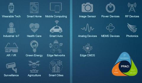
During an IoT, Comms, Auto, Power, Sensors (ICAPS) and Packaging Master Class, the company shared its view that evolving multi-billion unit markets would be enabled by enhancing semiconductor performance, lowering power, reducing area, and lowering cost (PPAC) (Figure 1.
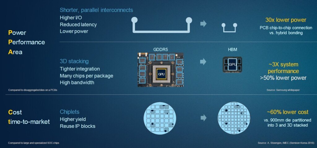
For decades PPAC, was enabled by monolithic semiconductor scaling that delivered simultaneous improvements in chip performance, power, and area/cost. Bust as classic scaling slows and becomes more expensive, chipmakers are moving towards heterogeneous design and in-package integration of chipsets and other devices to accelerate PPAC and time to market.
Historically, the primary function of packaging was to protect the die and connect it to the printed circuit board (PCB). It was regarded as the low-value, commodity part of the industry.
Recently, designers are rethinking how to best integrate both chips and systems. Heterogeneous design and advanced packaging are now a competitive imperative for the world’s leading semiconductor and systems companies. Multi-die advanced packaging instead of single-die packages mounted on a PCB enables high-performance logic and memory to be placed closer together to reduce latency and power consumption (Figure 2).
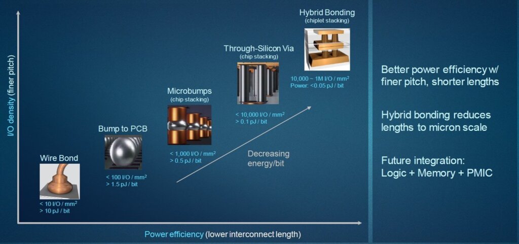
D2W hybrid bonding using direct, copper-to-copper interconnects to increase I/O density and shorten the wiring length between chiplets will improve overall performance, power and cost. To accelerate the development of this technology, AMAT says its is adding advanced software modeling and simulation to its Advanced Packaging Development Center. These capabilities allow various parameters such as material selection and packaging architecture to be evaluated and optimized prior to hardware development to significantly accelerate learning cycles and speed time to market for customers.
This builds upon the joint development agreement between AMAT and Besi to develop the industry’s first complete and proven equipment solution for die-based hybrid bonding (Figure 3)
Large Area Processing
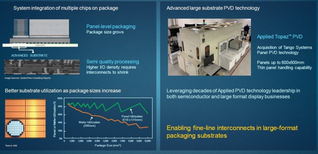
The need for larger package sizes with greater interconnect density is increasing as chipmakers squeeze greater numbers of chips into sophisticated 2.5D and 3D package designs. Applied is using state-of-the-art panel-level processing technology from its recent acquisition of Tango Systems. Panel-size substrates, which can measure 500mm x 500mm or larger, can accommodate a greater number of packages compared to wafer-size formats, thereby providing a cost-benefit in addition to better power, performance, and area. As its customers adopt these larger panel sizes, AMAT plans to provide them with access to large-area materials engineering technologies from its Display Group, including deposition, e-Beam testing, SEM review, and metrology and focused ion beam for defect analysis (Figure 4).
AMAT was one of the first front-end equipment suppliers to understand that packaging was becoming a more valuable approach to device fabrication as evidenced by their early entry into 2.5 and 3D IC packaging space as shown in Figure 5.
For all the latest in Advanced Packaging stay linked to IFTLE…………………..


