
Intel in Talks to Acquire GlobalFoundries
Trustworthy sources such as the Wall Street Journal are reporting that Intel is in talks to acquire GlobalFoundries (GF).
They report that the deal could value GF at around $30 billion. Talks appear to be directly between Intel and the Abu Dhabi government (which owns GF) since GF executives claim they are not in discussions with Intel. IFTLE will be watching this closely.
IFTLE thinks for Intel to acquire GlobalFoundries actually makes a lot of sense for reasons including:
- GF has been on the block for several years. Some have worried that China was trying to acquire it.
- Intel has announced a desire to compete head-on in the foundry business with TSMC and Samsung but industry experts (including IFTLE) have openly worried that the Intel “culture” made such an effort very difficult (in the true Japanese meaning of the term) , if not impossible.
- The US Government is rightly pushing “onshoring”, so what better solution than Intel becoming a powerhouse foundry business?
Intel / IBM Partnership
In other Intel news “IBM and Intel announced an important research collaboration to advance next-generation logic and packaging technologies. This collaboration aims to accelerate semiconductor manufacturing innovation across the ecosystem, enhance the competitiveness of the U.S. semiconductor industry and support key U.S. government initiatives.”
There was a time when they were both the very definition of the “leading edge”, being light years ahead of their competition, but not so much anymore. Both of them have, at times in their history, tried to open up their manufacturing to supply the industry, both in chip manufacturing and, in the case of IBM, packaging. Those have not been sterling successes either. While IBM has exited chip and package manufacturing totally, Intel has recently recommitted to their manufacturing and R&D roots. Hopefully, the remaining brainpower in both these companies can overcome their well-known arrogance and work together and put the USA back on top of these two very important industry segments……
Now, continuing our look at the 2021 ECTC Conference…
Samsung
Joonsung Kim and his coworkers at Samsung TSP (Test & System Packaging) discussed their work on “2.3D Packaging Solution using Fan-out Panel Level RDL”.
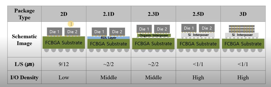
While IFTLE is NOT a big fan of the 2.1D and 2.3D nomenclatures (since 2.5D was a joke created by ASE intending to mean “not ready for 3D”) the community decides on what things are called, not me. We all agree that high-end applications need high-end packaging, and the table below shows how Samsung defines current packaging options.
Samsung is reporting in this presentation that they can achieve a 20 – 30% cost reduction by splitting the typical BGA substrate into two parts; (a) a coarse patterning substrate (40um L/S) and (b) a laminate substrate formed by fanout panel level RDL as shown in Figure 2.
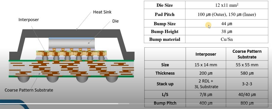
A cross-section of the real package is shown in Figure 3:
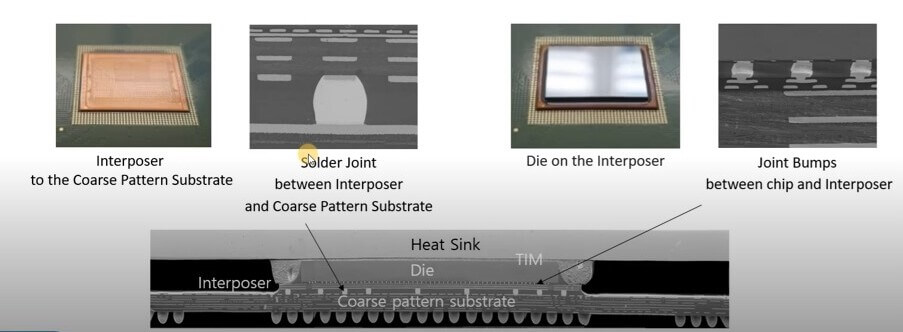
Figure 3: Actual package showing interposer attachment and die assembly, using the approach described in Figure 2. (Source: Samsung TSP)
Warpage issues were studied and resolved.

The interposer and the coarse pattern substrate were connected at 0.4mm pitch; the solder joints between the chip and the interposer were at 100µm pitch. The warpage of the final package with heat sink was 93µm convex.
MJ Kim of Samsung TSP detailed the company’s work on “2.5D RDL Interposer Packaging”. Its 2.5D RDL first silicon interposer package was fabricated as shown in Figure 4. The interconnect consists of 2µm L/S and 55µm micro bump attach.
Figure 4: RDL-first process flow for achieving Samsung’s 2.5D RDL interposer package. (Source: Samsung TSP)
They demonstrated 2.3Gb/sec/pin with the HBM. Such packages passed all system-level reliability testing.
Murata
Funaki of Murata presented the work they have done with the Tokyo Institute of Technology, DISCO, and ITRI on miniaturized 3D functional interposers using bumpless chip-on-wafer (CoW) integration with capacitors. Basically, their premise is that capacitors are taking up too much room on 2.5D interposer module assemblies so they have developed technology to bury the capacitors into the silicon interposer as shown in Figure 5. This results in a shorter interconnect length and smaller module area.
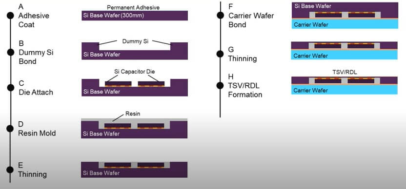
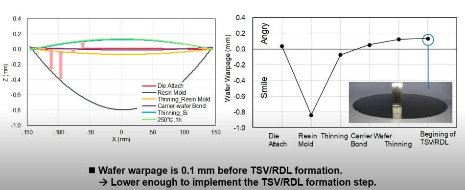
The most significant issues in the overall process were the die attach and resin molding steps which result in void (adhesive voids cause die movement) and warpage issues, respectively. Wafer warpage after the RDL step should be no more than 0.3mm. Warpage vs process flow is shown in Figure 6.
RDL with 10um TSV results in significantly lower parasitic capacitance due to the shorter interconnections.
For all the latest in advanced packaging stay linked to IFTLE………………………………….


