Approximately 880 people registered for IMAPS International 2013, and yes the fiasco in Washington even affected IMAPS – there were last minute cancellations from people who work directly or indirectly for the government. But I was there, and here are the highlights: Qualcomm : Vidhya Ramachandran presented data on a prototype 3D memory on logic package. The paper was co-authored with TSMC. Yup, it wasn’t interposer based, it wasn’t a package-on-package (PoP), but based on TSV interconnects. The logic chip contained TSMC’s 28nm high-k metal gate process and connected to a 4Gb Wide I/O DRAM with a 40µm pitch JEDEC Interface. Ramachandran also laid out a well-defined process flow that included optional intermediate points for testing devices. The memory device to logic connect would be a front to back attach on to the Logic chip, with the back of the logic chip containing the Wide IO Memory interface. In order to ensure connectivity from the front of the logic chip to the back. The various test points included probing the micro-bump on the back, probing on film-frame, partial stack-test and final test. This definition of test points is key to get the industry to line-up behind all the different permutations and combinations of test points that could be conceived in for a full stacked die process flow. 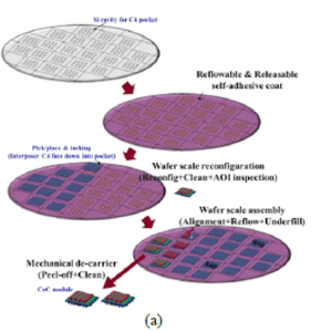 Xilinx : Any TSV seminar would not be the same if we did not hear from Xilinx. This time Woon-Seong Kwon from Xilinx discussed their twist on the re-configurable chip-on-wafer (COW) interposer technology. While previous presentations from Xilinx focused on the BEOL area of the front-end and the impact of the large die-partitioning into 4 smaller dies to improve wafer yield, this award-winning paper focused on the re-configurability in the back-end to improve back-end yield. Directly attaching a chip to a warped interposer can reduce yield and increase risk of damage from warpage. A number of factors contribute to the warpage, Front-side Cu process, TSV features, processing temperatures and from different dielectric film-stack on both sides of the wafer. Instead of attaching a die directly onto an interposer wafer, the interposer wafer is singulated, and using a die-placement machine, die are transferred from film-frame onto a silicon wafer with pockets. The re-configurability has the added benefit of allowing interposer clean and inspection to take place at a wafer–level. There are over 200,000 micro-bumps/wafer and defects from contamination quickly kill final package yield. By re-configuring into a wafer, both the inspection and clean are at a wafer level. GLOBALFOUNDRIES: David McCann gave an interesting keynote talk on the supply chain for 2.5D and 3D. Industry seems to be triangulating towards a clean break between the front-end TSV and via formation capability with the middle-end-of-line (MEOL) handling thinning, dual-sided bumping and RDL. This ensures that the hand-off between the foundry and the MEOL is a full thickness wafer with none of the risk associated with transporting thinned wafers. GF calls it the Open (Collaborative) model. The current state of the art is that the Interposer cost is nearing HVM cost requirements, but the cost is highly dependent on the design. Bond/de-bond COO and Yield are still a bottleneck. For larger interposers warpage management remains key. And a cost-effective probe strategy is required for 40µm/50µm pitch. This echoed Vidhya’s presentation and the proposed testing strategy. McCann went on to say that GF is a reluctant interposer supplier. GF is building interposers on a 65nm line. Clearly overkill for 2um line spacing and width. He made the point that someone with a line balanced and optimized for interposers will probably produce the lowest COO interposers.
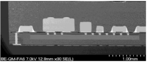
Infineon: Infineon was a pioneer in the fan-out package development and commercialization with their successful eWLB package. Since then Intel Mobility (carve out from Infineon) , STATS-Chippac, Nanium, and ASE have also been shipping eWLB packages primarily for mobile applications. Klaus Pressel presented examples of both side-by-side and stacked package applications of eWLB, where essentially the fan-out area acts as an interposer. The vias – through encapsulant vias (TEV) are made using a laser drill and electroplated with Cu, connecting both sides of the package with RDL layers also on both sides. The examples shown had passive devices stacked on die. This was an good example of the viability of eWLB to be a platform for interposer applications. 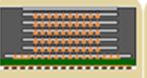 Micron and Hynix: Both Micorn and Hynic presented the true 3D TSV based interconnect stacked memory packages – Micron’s Hybrid Memory Cube and Hynix’ high bandwidth Memory. Bottom most layer for both is an interposer. The goal is an all Si cube. Applications for these are for servers. High volume production is expected to commence mid 2014. Panel discussion on TSV challenges: Rich Rice of ASE, Matt Nowak of Qualcomm, and Raj Chelani a consultant, were on the panel discussing challenges to 2.5D and 3D HVM. My key take-away – a bulk of the core technology issues have been resolved. We know how to etch, fill, thin, bond, de-bond and build cu pillar bumps and RDL. Yes there are still some yield issues especially at de-bond. Equipment is slow and expensive. But in general, we know how to put devices together as a 2.5D or as a 3D stack. Matt used to talk about a $2 interposer, he gave a bit more specificity when he issued the challenge for a <1c/sq mm for interposer with the ability to go down to 2µm line space and line width. There was unanimous agreement that people didn’t care about the material – whether it was Si, or glass or organic. Yields and the resulting cost were the key drivers for commercial viability. Supply chain business models were in place as was noted in the GLOBALFOUNDRIES presentation. Hard evidence of the ability to meet cost and performance goals were the only to see large scale adoption. Over the years we have seen evidence of bits and pieces of the 3D package being discussed and how theoretically 2.5D and 3D were just round the corner. With presentations from Qualcomm, Xilinx, Micron and Hynix, there was a lot more evidence that fully characterized 2.5D and 3D solutions will be making their production debut in 2014. Exciting times no doubt. I would be remiss if I did not congratulate my colleagues from Rudolph Technologies – Jim Webb and Russ Dudley who won best paper awards in their respective tracks – Jim for the advanced package stepper for wafers and panels, while Russ won his for an integrated Inspection and metrology solution for TSV. ~ R.R.