
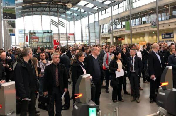
SEMICON Europa was an island in the vast sea of Electronica. It occupied one hall out of 18. But without that hall full of equipment, process, and material suppliers, the other 17 wouldn’t have any reason to exist. Think about that for a bit. There’s a reason “Semiconductors drive smart” was SEMI’s chosen theme for the event.
Rather than attend all the sessions in the tech arena, I chose to spend my time chatting with the exhibitors in hall A4. In comparison with last year’s event, which was co-located with Productronica, they reported less foot traffic, attributing it to hall’s location. Last year, all visitors had to walk first through SEMICON Europa before getting to the Productronica exhibit halls.
While Electronica was a better match to tell the supply chain story, most exhibitors I spoke with felt that from a customer perspective, they are more aligned with the Productronica exhibitors than Electronica exhibitors.
Powered by Optical Sensors
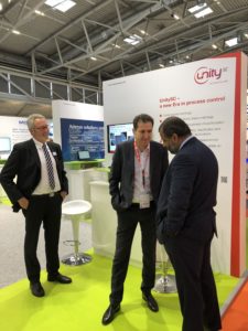
Kamel Ait-Mahiout, CEO of UnitySC, was one of those who was pleased about the event’s co-location with Electronica, as it provides attendees with more of the supply chain. He talked about the company’s latest tool introduction, the UnitySC Light-IX, which is the first platform to implement technology gained as a result of the HSEB acquisition early in 2018. It’s also part of the company’s overall strategic plan to cover a broader scope of inspection and metrology needs with fewer platforms.
This first-generation Light-IX platform was conceived to fill a gap for today’s outsourced semiconductor assembly and test (OSAT) suppliers. Ait-Mahiout said that as wafer level packaging feature sizes continue to decrease, OSATS need inspection systems for high volume manufacturing that can detect defects in bumps, micro-bumps, and redistribution layer (RDL) down to 2µ l/s.
This “tool that sees everything” uses new illumination optical sensors combined with proprietary algorithms to detect things like shorts and opens on RDL and residues on bump top and bond-pads that lead to field failures. Designed for HVM environment, the system can be configured to inspect wafers up to 300mm, including thin wafers, reconstructed wafers, and wafers mounted on dicing frames.
While the tool is targeted to the back-end,Ait-Mahiout says the company will “touch the front end” with the same tool.
Round Peg, Square Hole
In fan-out panel level packaging applications, one of the identified pain points is in the lithography steps for patterning the RDL layers. In particular, depositing lift-off layers thinly and uniformly on a rectangular substrate is a challenge yet to be solved by spin-coating. People were using slit coating, which doesn’t create a thin or uniform enough layer for the lift-off layer.
In the Obducat booth, CEO Patrik Lundström and his team showcased the company’s solution to this issue: a spin coater that uses rotating cover chuck technology (RCC) to spin coat uniformly on square substrates up to 1.5m in diameter, at a target thickness of ~ 500nm.
The key is to avoid turbulence during the spin process to reach a thinner and more uniform coat and have the same amount of material in the center as at the corners, with only a 5-10mm edge exclusion, explained Lundstrom. The rotating covered chuck allows for that to happen.
Lundstrom said Obducat, based in Switzerland, supports both the front-end and advanced packaging markets. It provides lithography support tool for the steps leading up to and following lithography, including clean, coat and bake, as well as nano-imprint patterning, wet etch, strip, bonding and debonding. The company has seen an uptick in the last year in interest in the wafer-level packaging segment.
3D InCites Success Story
I stopped by Gemark Automation’s to check out the second generation of its beer pouring robot, which I’m happy to say has shaved 8 seconds off its time from generation one.
Is it beer thirty yet? Stop by Nidec at booth A4.659 to enjoy a perfectly poured Hefeweizen. Tell Karl we sent you. #SEMICONEuropa @SEMIEurope pic.twitter.com/fhUn1D3W8U
— 3D InCites (@3DInCites) November 15, 2018
A Genmark robot was also being demonstrated as a transport system for glass substrates in temporary wafer bond/debond systems.
Robots for automatic beer pourers are just a side gig for Genmark Automation. Also on display last week at #SEMIEurope was its wafer handling robot. @SEMIEurope pic.twitter.com/1H0b4VO7s6
— 3D InCites (@3DInCites) November 20, 2018
It handles the glass wafer while it is being inspected for thickness and uniformity, so that compromised glass wafers can be detected and discarded. This leads to improved yield. The company is also looking into non-standard substrate handling, varying from 6-inch wafers to large format panels and everything in between.
But that wasn’t the only good news Carl McMahon, EVP worldwide sales and marketing had to share. He said that as a direct result of exposure from this 2015 article posted on 3D InCites, five Codex stocker and storage systems have shipped in the advanced packaging market. He expects to hit double digits with the number of systems shipped by 2020.
The company was recently acquired by Nidec, a Japanese company listed on the Nikkei stock exchange. Now a wholly owned subsidiary of Nidec, Genmark retained its brand but gave it a facelift. Being part of a publicly traded company has increased customer confidence in Genmark’s longevity.
“This is opening up new markets for us in Asia and is allowing us to increase product development in the advanced packaging market,” noted McMahon.
Genmark is expanding its presence in Europe, opening a global repair center in Neufahrn, Germany, near the Munich airport. It will be equipped to repair all products worldwide for all customers. A dedicated center of excellence, McMahon says all technicians have an average of 15 years of experience. The team will work on upgrading and identifying newer technology that enhances repair and increases the life of the product.

15 Years and Growing Strong
Celebrating its 15th anniversary at SEMICON Europa seemed only fitting for European tool supplier, Trymax. Base in the Netherlands, the company specializes in plasma-based ashing tools for photoresist removal, isotropic etching, and photoresist pretreatments.
I caught up with Yann Guillou, who recently joined the company to run its sales and marketing efforts. He reported that the company is growing by leaps and bounds, not just in Europe, but in the US, China and Taiwan as well. from 20 to more than 60-79 employees in the past three years. To address a broader market and extend its reach into the US, Trymax has engaged Plasma-Therm as its US distributor.
A full-scale model of the NEO3400 300mm 4-chamber advanced ashing tool was on display. This tool supports support fan-out wafer level packaging and MEMS applications.
Come check out Trymax’s cool new NEO3400 300mm 4-chamber advanced ashing tool. Booth A4.237. Tell them we sent you! # #SemiEuropa @TweetTrymax pic.twitter.com/7zEqnJiJ5H
— 3D InCites (@3DInCites) November 15, 2018
A Year of Acquisitions
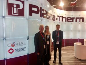
In the past year, Plasma-Therm has been busy establishing a strong presence in Europe by acquiring KOBUS for its fast atomic sequential technology (F.A.S.T) platform and Corial, suppliers of etch and deposition tools, for its R&D expertise. These strategic moves extend Plasma-Therm’s portfolio of plasma etch, deposition, and singulation tools, as well as its global footprint.
I spoke with Thierry Lazerand, who just wrapped up his position as director of marketing at the Florida headquarters, to return to his hometown of Grenoble, and lead the sales and marketing effort at its new European facility.
According to Lazerand, KOBUS has been absorbed into Plasma-Therm, but its name lives on as a product line. Corial exists as a wholly owned subsidiary of its new parent company and will serve as Plasma Therm’s R&D arm and equipment supplier for research labs, universities, and low-volume producers. Its facility will serve as the European presence for Plasma-Therm.
“The idea is to be in direct connection with European R&D markets, as well as emerging markets like compound semiconductors and all heterogeneous integration touch points,” says Lazerand.
The acquisition of these companies plays directly into Plasma-Therm’s strategy to participate in the European advanced packaging initiative. The company’s collaborative spirit and longevity among its employees is what makes it unique and a good fit for Grenoble explained Lazerand.
“We never crushed a company to take its IP,” he said. “Rather, we focus on investing in them for the products and make them better.” They focus acquisitions on plasma-based equipment and then form partnerships with adjacent technologies if there is an advantage. For example, plasma dicing is done in partnership with Disco. Another example of this is the US distribution agreement with Trymax.
A Word on Hybrid Bonding
My last stop was at Besi, to capture its Datacon 2200 evo high-accuracy die bonder in action. Perfect for system-in-package applications.
Stop by booth A4.351 and check out Besi’s Datacon 2200 evo high-accuracy die bonder. Perfect for #SiP. Tell them we sent you. #SEMICONEuropa @SEMIEurope pic.twitter.com/sxtD9RsJLx
— 3D InCites (@3DInCites) November 15, 2018
I wanted to talk about die-to-wafer bonding activities using hybrid bonding instead of thermocompression bonding, because of the presentation I attended at last year’s ECTC 2018 frontiers in assembly session.
According to René Henricks, senior VP of sales, the first machines are being shipped, but hybrid bonding is still in very early stages. Thermocompression bonding is still the mainstream and comprises the majority of Besi’s install base, he said. However, there’s lots of discussion about hybrid bonding with the company’s high-end customers. He added that to meet today’s fine pitches in high volume manufacturing, there is interest not only in the bonding technology itself but also high accuracy placement in a clean environment.
Over to Electronica
A walk into the next hall showed us how advanced packaging, enabled by all the latest tools, processes and materials, are being put to work in new applications. Check those out here. ~ FvT


