
Through-silicon vias (TSVs) have been firmly established as a method of interconnect that enables high bandwidth and low latency between dies at extremely low power dissipation. Used for years in microelectromechanical systems (MEMS), compound semiconductors, and image sensors, TSVs are now also in mainstream production for 2.5D interposer technologies, and for stacking die to create high-bandwidth memory (HBM) in a true 3D IC architecture.
For a while, it seemed like 3D ICs using TSVs would be forever relegated to low-volume production for high-performance computing (HPC) applications like gaming, network devices, and servers, due to the high cost of production. There always seemed to be a lower-cost alternative, such as fan-out wafer level packaging (FOWLP), to provide the level of interconnect density required to do the job. Recently, however, TSVs are regaining popularity as 5G, artificial intelligence, machine and deep learning applications call for interconnect density that only they can provide.
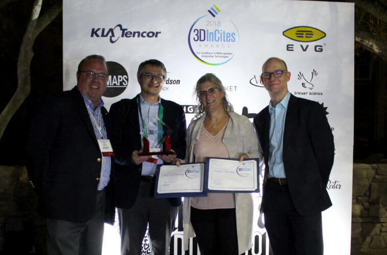
As part of our 2018 3D InCites Award Winner series, we spoke with Julien Vitiello, CEO of the former KOBUS (now part of Plasma-Therm), about why the industry needs lower-cost TSVs and how to get them.
Why we need Low-cost TSVs
Vitiello says that because of the increased need for new applications in smartphones, there’s lots more interest in integrating MEMS, RF devices, and power devices into them. This requires more adapted solutions such as fan-out and TSVs. It’s no longer a choice between FO and 3D TSV stacked ICs. These technologies will co-exist based on the benefits each provides.
“3D never left the scene,” noted Vitiello. “What we’re seeing now is the next big wave where 3D TSVs are becoming more and more important.”
Moreover, noted Vitiello, the reality is that the high-volume manufacturers with 300mm lines can’t provide everything. It’s less about high volumes of TSV devices and more about a wider variety of devices in small volumes. This is providing an opportunity for second-tier players who manufacture 200mm wafer sizes and below, as well as for the rest of the ecosystem.
Why TSVs still cost so much
According to Vitiello, one reason the cost of TSVs is so high is that, as leading foundries and integrated device manufacturers add capacity for finer technology nodes, they are leveraging older toolsets to manufacture TSVs, rather than buying tools designed specifically for TSV processes.
For example, deposition processes performed on tools that have not been optimized for TSVs end up taking longer, require many layers to achieve conformal coating and meet constraints, and also end up needing a longer chemical mechanical planarization (CMP) step.
Vitiello said in his experience with atomic layer deposition and electroless plating processes, requiring new chemistries becomes a challenge because companies are afraid to introduce new materials into the CMOS stack. They find a technology that works and don’t want to move to the next one.

“We see people living with that in terms of cost,” said Vitiello. “If they want to shrink devices and achieve a new form factor, they have to reduce dimensions or increase the aspect ratio. Because working with thinner substrates requires additional steps, they prefer to stay at 200-300µm rather than going to 50µm.”
Solving the issue
From Vitiello’s perspective, the solution to reduce TSV cost is simple: buy a tool that makes other integration steps easier, thereby reducing the overall cost of the TSV. “If you use tools developed specifically to meet TSV constraints, you’ll facilitate other integration steps and save money at the end.”
Plasma-Therm’s KOBUS deposition tools for TSVs feature its proprietary fast atomic sequential technology (F.A.S.T.) to combine the performance of ALD at chemical vapor deposition speeds, explained Vitiello. “Our technology can define conformality of the top, sidewalls, and bottom of the TSV,” he said. “We work on integration and not only the process itself.”
Moving Forward
As a start-up, KOBUS won the 3D InCites Start-Up of the Year award in 2017 and 2018. In 2018, the company’s F.A.S.T technology also won Process of the Year. Since the awards were presented in March, Plasma-Therm acquired the company, adding the tool line to its portfolio of plasma etch, dicing, and PECVD tools targeting specialty markets with small players. Vitiello explained that as a small French company, they needed a partner to help them grow. KOBUS filled in the gaps at Plasma-Therm with its ALD tools and complementary technologies.
“It’s a good fit,” says Vitiello. “We share the same feeling and spirit, how we want to work with customers, which markets to address.”
Vitiello says the company is not focused on serving the mainstream TSV market but is eager to support those smaller players looking for lower-cost TSV solutions to take advantage of the new markets looking to integrate TSVs into their devices.

